
Key Takeaways
zynqmp-hailo-aiis an open-source (MIT) reference design from FPGA Developer / Opsero that pairs a Zynq UltraScale+ MPSoC with a Hailo-8 AI accelerator for multi-camera YOLOv5 vision.- Up to four Raspberry Pi cameras feed independent MIPI CSI-2 pipelines in the PL: capture, Vitis Vision ISP, scaling and color conversion, then DDR frame buffering.
- The Hailo-8 does not run on the ARM cores. It sits behind a PCIe Gen3 link (x1 or x4) and the PS reaches it through an XDMA block configured as a PCIe Root Port in AXI Bridge mode.
- YOLOv5m runs at roughly 150 FPS, and the figure barely changes between Gen3 x1 and x4 — the bottleneck is the accelerator’s own compute, not link width.
- The display path is complete too: a video mixer composites up to four camera layers plus RGBA overlays and outputs 1920×1080@60Hz over DisplayPort.
In one line: once you add cameras to an FPGA vision project, complexity climbs fast — how do you capture several MIPI CSI-2 streams in parallel, run ISP, move all that video through DDR, and still hook up AI inference over a high-speed link? The zynqmp-hailo-ai project answers all four questions in one buildable design, and Aomway walks through the architecture, the PL video chain, the PCIe plumbing and the real throughput numbers below.
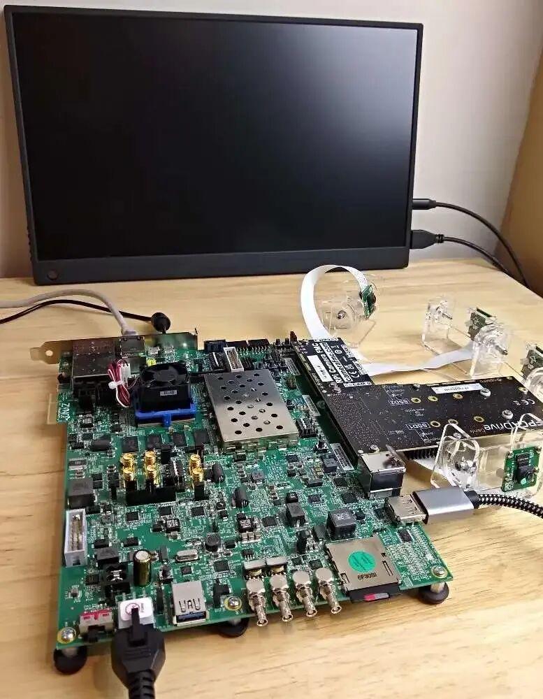
The project comes from FPGA Developer (Opsero), the same group behind the widely used fpgadeveloper reference repositories. It is a reference design that combines an AMD Zynq UltraScale+ MPSoC with a Hailo-8 AI inference accelerator to deliver real-time multi-camera YOLOv5 vision processing.
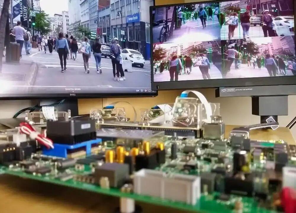
The design accepts up to four Raspberry Pi cameras. The FPGA programmable logic handles MIPI capture, ISP, video format conversion and frame buffering, then hands data to the Hailo-8 over PCIe for AI inference, and finally displays the multi-camera video with detection results on screen.
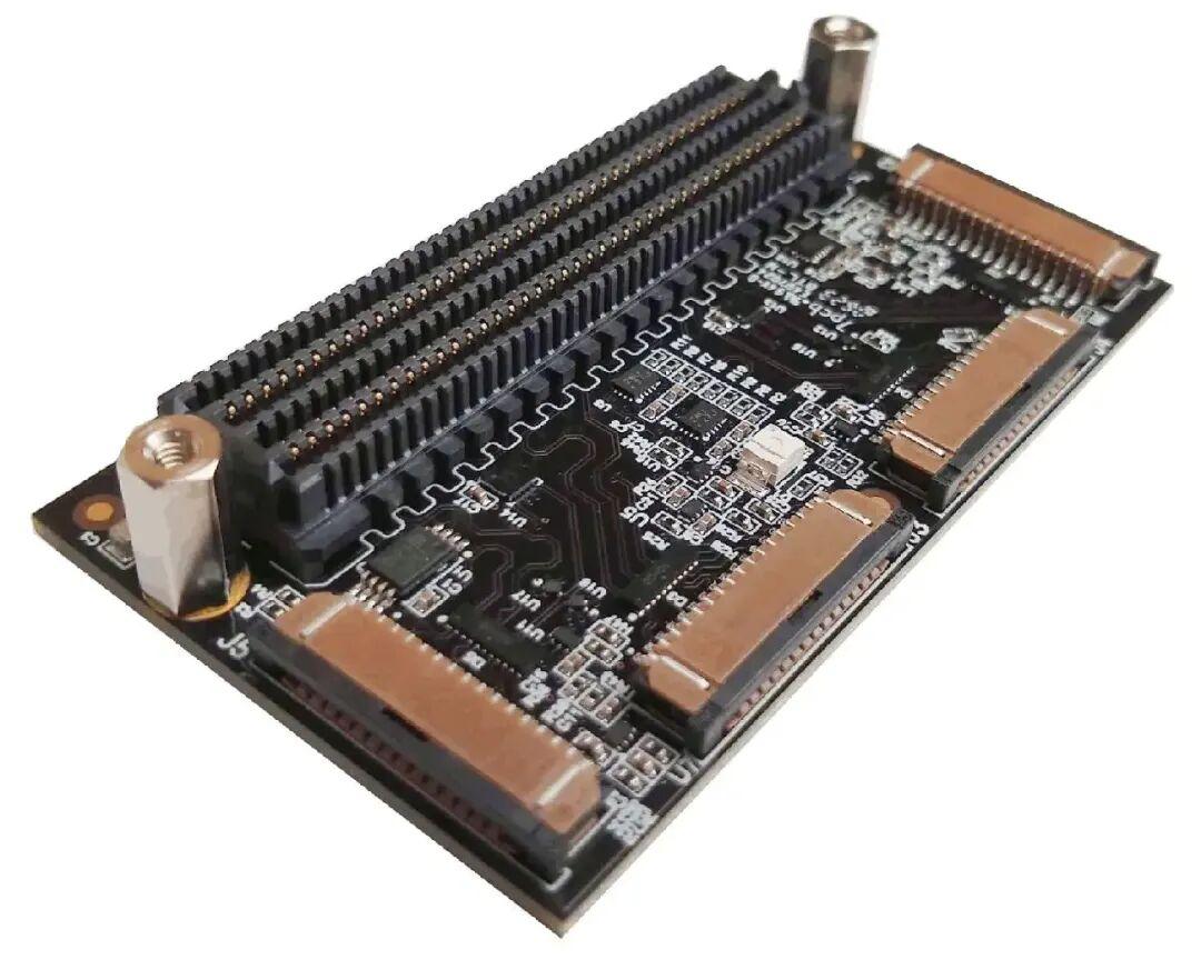
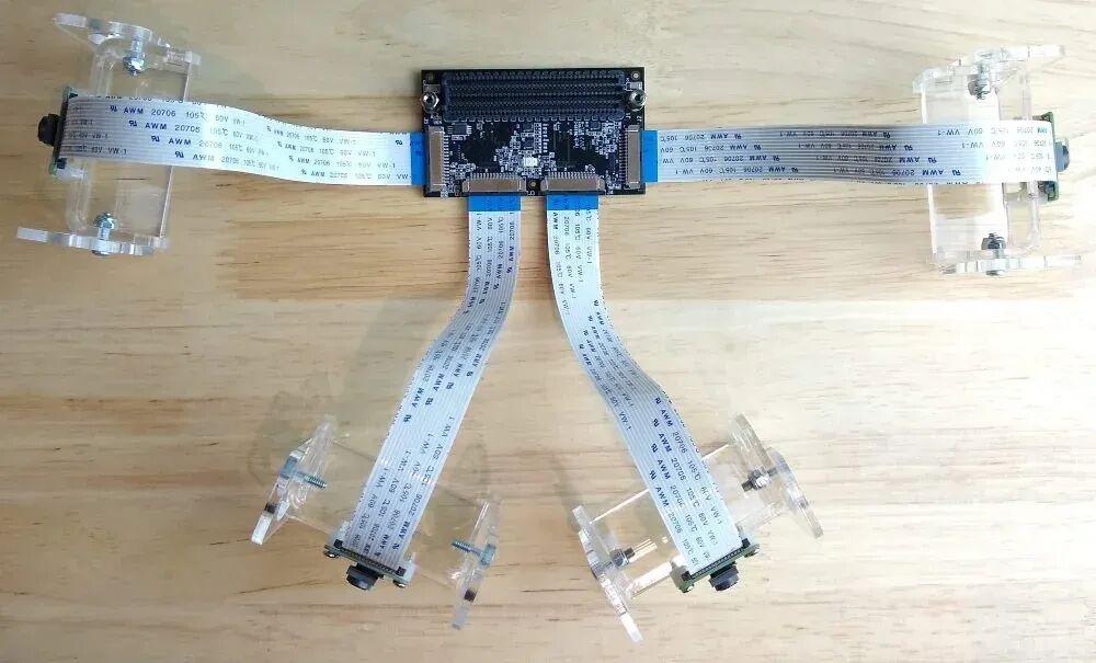
The repository ships more than a Vivado hardware project: it includes PetaLinux and Yocto build files as well as the runtime scripts, which makes it a solid reference case for anyone studying FPGA + AI co-processing architectures.
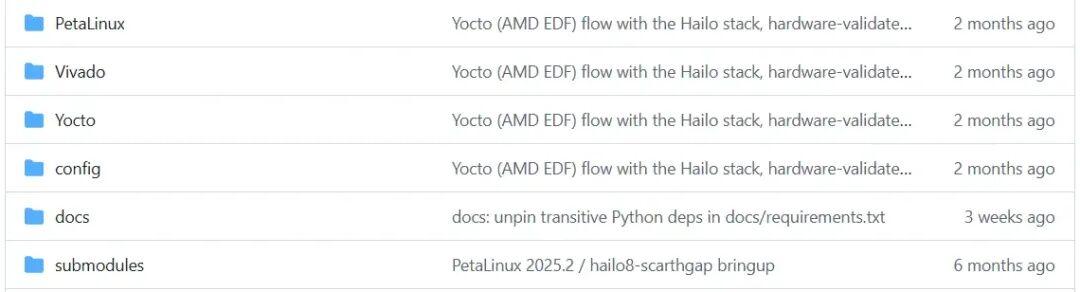
Project: github.com/fpgadeveloper/zynqmp-hailo-ai
Hardware Architecture: FPGA Plus AI Accelerator
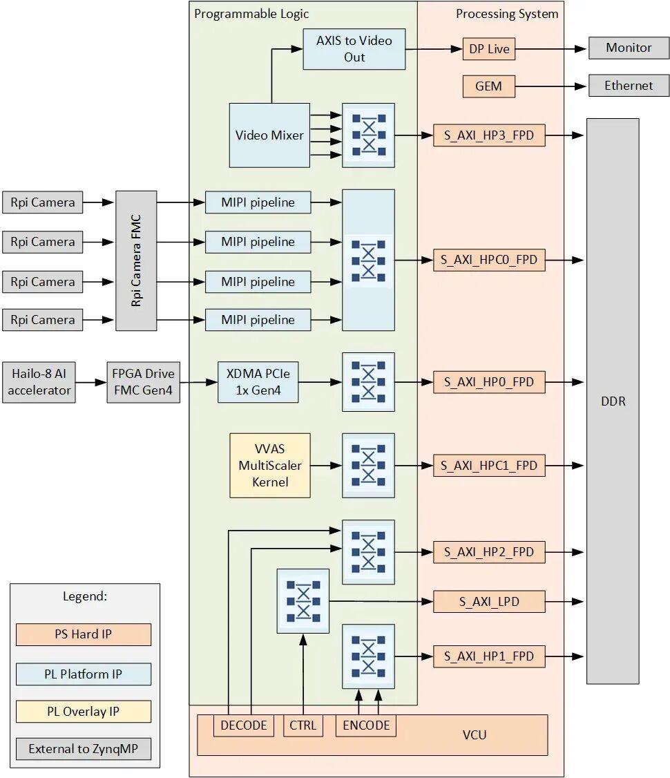
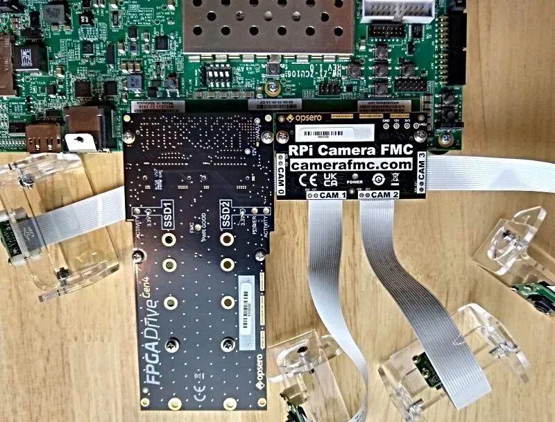
The core idea is clean: let the FPGA handle real-time video data processing, and let a dedicated AI accelerator handle neural network inference. The system has three parts.
- Zynq UltraScale+ MPSoC — multi-camera capture, ISP image processing, video buffering, display output and overall system control.
- Hailo-8 AI accelerator — connected to the FPGA board through an M.2 interface, dedicated to YOLOv5 inference.
- Multiple Raspberry Pi cameras — up to four, providing parallel image input.
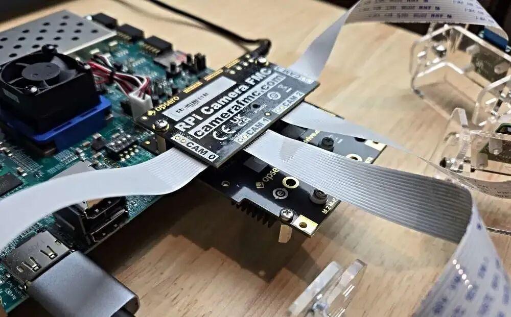
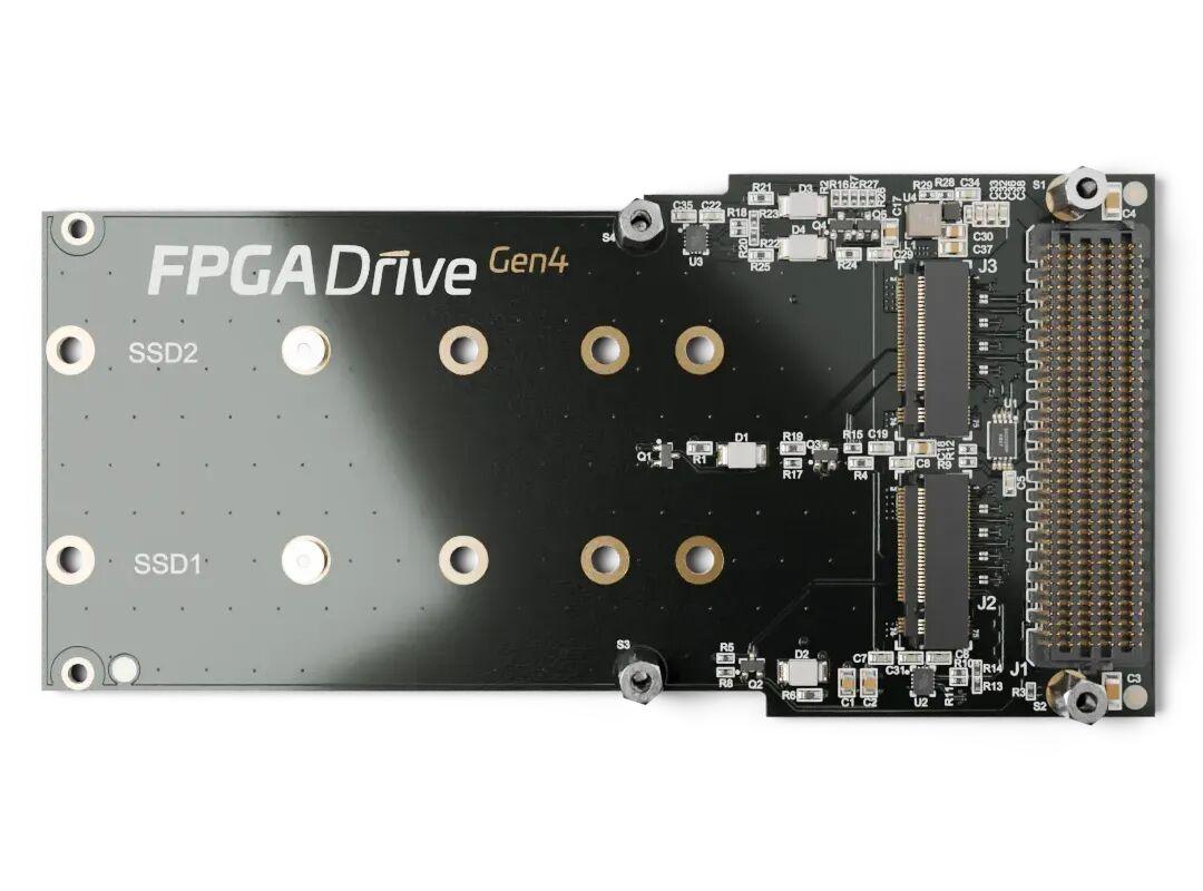
The cameras attach to the ZynqMP through the Opsero RPi Camera FMC expansion card, while the Hailo-8 attaches through an FPGA Drive FMC Gen4 or M.2 M-key Stack FMC card.
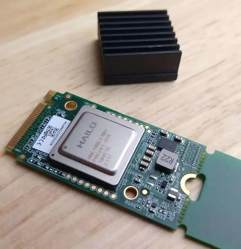
One design decision is worth flagging: AI inference does not run on the ZynqMP ARM cores. The compute task is handed to an external Hailo-8 over PCIe. That gives you a genuinely heterogeneous platform, with the programmable logic, the ARM processing system and the dedicated AI accelerator each doing what it is best at.
FPGA PL Side: A Complete Multi-Camera Video Chain
For FPGA developers this is the most instructive part of the project. Each camera gets its own independent capture and processing channel, built from five IP blocks:
- MIPI CSI-2 Receiver Subsystem
- AXI4-Stream Data FIFO
- Vitis Vision ISP Pipeline
- Video Processing Subsystem
- Frame Buffer Write
The overall flow is:
MIPI CSI-2 → AXI4-Stream → ISP → video scaling / color conversion → DDR frame buffer

MIPI CSI-2 Capture
The system receives image data from the Raspberry Pi cameras through the MIPI CSI-2 RX IP. Each camera uses two MIPI data lanes, and the receiver outputs RAW10 video as AXI4-Stream. All four cameras get their own capture channel rather than being serialized into one, which is the right call: independent data paths make it far easier to organize capture and buffering for each stream.
Vitis Vision ISP
RAW10 data enters the Vitis Vision ISP Pipeline (the reference implementation lives in the Vitis_Libraries vision examples), which performs a series of basic image operations:
- BPC — bad pixel correction
- Gain control
- Demosaicing
- Auto white balance
- Gamma correction
After ISP the image goes from RAW10 to RGB888. The Video Processing Subsystem then handles scaling and any required color space conversion.
One detail is worth noting: the design does not dump raw camera data straight into the AI model. It first finishes image preprocessing in the FPGA and organizes the data into the form downstream stages want.
Better still, some ISP parameters can be changed at runtime through the Linux V4L2 control interface — per-channel gamma, gain and white balance thresholds. That means tuning image parameters does not require regenerating the FPGA bitstream.
DDR Frame Buffering
Once processing is done, the Frame Buffer Write IP writes video into DDR. DDR carries a lot of weight in this system: it holds frames from all cameras, supplies input data for AI inference, feeds the display channel, and lets multiple processing modules share data. In any multi-camera system, DDR bandwidth, buffer organization and read/write arbitration are the things that decide whether the design actually holds up.
PCIe: Connecting the Hailo-8
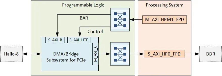
This is the other part of the project worth studying. The Hailo-8 is not attached through GPIO or a slow peripheral interface — it plugs into the FPGA platform through an M.2 socket and communicates over PCIe Gen3.
The Vivado project instantiates AMD/Xilinx’s DMA/Bridge Subsystem for PCI Express (XDMA) and configures it as a PCIe Root Port operating in AXI Bridge mode. Depending on how many GT lanes the board’s FMC interface exposes, two PCIe configurations are supported:
- PCIe Gen3 x1
- PCIe Gen3 x4
ZCU104, PYNQ-ZU and the standard zcu106 design use a Gen3 x1 link; zcu106_hpc0 and uzev support two Gen3 x4 PCIe Root Ports. Those two designs can also use the second M.2 socket for a second Hailo-8 or an NVMe SSD.
There is a nice engineering detail here: the project explicitly handles PCIe BAR address mapping. The PS reaches PCIe devices through the Root Port’s AXI BAR window, which is placed at 0xB000_0000; in dual-Root-Port designs each port gets 128 MB. This also fixes a problem in earlier versions where an NVMe SSD in the second M.2 socket would fail to enumerate.
For anyone working on ZynqMP PCIe Root Ports, XDMA, AXI Bridge and Linux PCIe drivers, this part alone is worth reading.
Multi-Camera Compositing and DisplayPort Output
Beyond AI inference, the project implements a full video display path.
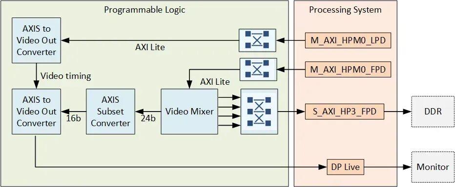
A Video Mixer composites the camera images — up to four camera layers, plus RGBA overlay layers. It reads the different video layers from DDR, scales and blends them, then outputs to the ZynqMP PS DisplayPort live video interface. The display subsystem consists of:
- Video Mixer
- Video Timing Controller
- Clocking Wizard
Final output is 1920×1080@60Hz with a pixel clock of 148.5 MHz. On the Linux side the DRM driver controls the mixer’s display mode, and the clocking module generates the matching pixel clock.
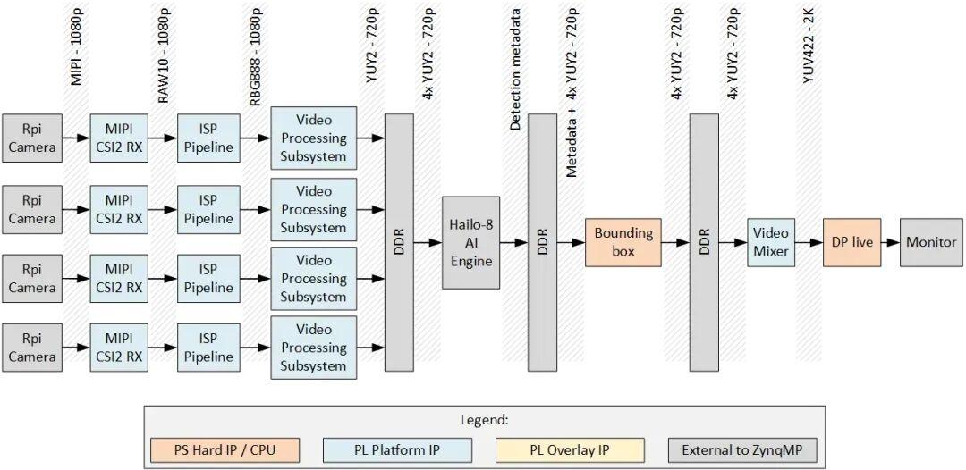
So this is not merely a camera capture accelerator. It covers the whole chain: image input, processing, AI analysis and multi-window display.
AI Throughput: About 150 FPS on YOLOv5m
On the AI side the project runs a YOLOv5m model on the Hailo-8. According to the project documentation, the YOLOv5m network supplied with the design runs at approximately 150 FPS on the Hailo-8.
Notably, the documentation states that the figure stays at about that level under both PCIe Gen3 x1 and Gen3 x4 link configurations — the bottleneck is the Hailo-8’s own compute capability, not PCIe link width. The lesson generalizes: in a real heterogeneous system, more PCIe bandwidth does not automatically buy faster inference.
The software side is fairly complete as well, shipping:
- HailoRT runtime
- Hailo PCIe driver
- Hailo GStreamer plugins
- YOLOv5m HEF model
- Camera initialization and display scripts
- Multi-camera AI demo scripts
hailodemo.sh is the main entry point for running the multi-camera AI demo.
One caveat: 150 FPS is the accelerator performance figure quoted in the project documentation for YOLOv5m. It does not mean all four cameras each run at 150 FPS. Real system throughput also depends on camera input frame rate, image preprocessing, data transfer and inference scheduling.
Supported FPGA Boards
The project provides reference designs for several Zynq UltraScale+ platforms.
| Board | Cameras | PCIe configuration | VCU |
|---|---|---|---|
| ZCU104 | 4 | Gen3 x1 | Supported |
| ZCU106 | 4 | Gen3 x1 | Supported |
| ZCU106 HPC0 | 4 | 2× Gen3 x4 | Supported |
| PYNQ-ZU | 2 | Gen3 x1 | Not supported |
| UltraZed-EV | 4 | 2× Gen3 x4 | Supported |
PYNQ-ZU implements only two camera channels because of device resource limits. ZCU106 offers two different hardware designs:
zcu106— the camera FMC and the PCIe expansion card occupy HPC0 and HPC1 separately.zcu106_hpc0— uses the M.2 M-key Stack FMC, stacking the camera card on top of the M.2 card, occupying a single FMC interface while supporting two M.2 sockets.
Boards that support VCU also integrate the ZynqMP’s internal video codec unit into the hardware design. The upshot is that one reference design can be trimmed and extended according to each board’s interfaces and resources.
Building the Project
The repository provides fairly complete build scripts, so you do not have to construct the Vivado block design from scratch. The current main branch targets the AMD/Xilinx 2025.2 toolchain and covers Vivado 2025.2, Vitis 2025.2, PetaLinux 2025.2 and the AMD Embedded Development Framework (Yocto).
Clone the repository first:
git clone --recursive https://github.com/fpgadeveloper/zynqmp-hailo-ai.git

cd zynqmp-hailo-ai
Be sure to use --recursive — the project contains Git submodules.
The build is driven by a single Python script, build.py, with Windows and Linux entry points.
1. List supported targets
./build.sh list2. Generate the Vivado project, bitstream and XSA — ZCU104 as an example:
./build.sh xsa --target zcu1043. Build PetaLinux
./build.sh petalinux --target zcu1044. Build the Yocto system
./build.sh yocto --target zcu1045. Build everything at once
./build.sh all --target zcu104Or build every supported target:
./build.sh all --target allThe script detects the Vivado, Vitis and PetaLinux installations automatically and runs the stages in dependency order.
Two practical constraints: PetaLinux and Yocto builds require a Linux environment — Windows can run the Vivado portion but cannot complete the full Linux system build. And a full build is resource-hungry: the documentation recommends at least 32 GB of RAM and about 40–50 GB of disk space per platform, with the first complete build potentially taking hours.
What’s Worth Borrowing From This Design
The most valuable thing here is not any single IP block or AI model, but the mature FPGA + AI system design pattern it demonstrates.
First, the FPGA owns the data path and the AI accelerator owns the compute. Camera data enters the PL, runs through a hardware pipeline for capture, ISP, format conversion and buffering, then talks to the accelerator over PCIe. This exploits the FPGA’s parallel processing while keeping heavy neural network inference off the ARM CPU.
Second, video processing and AI inference are not isolated modules. The project chains MIPI, Vitis Vision, DDR, PCIe, GStreamer and DisplayPort into one complete application system. For industrial vision, intelligent surveillance and multi-camera detection work, that system-level reference is usually worth more than a standalone algorithm demo.
Third, both hardware and software engineering are open. From the Vivado block design to PetaLinux and Yocto, then the Hailo driver and application scripts, the project supplies a fairly complete engineering foundation. Developers can build on it to study PCIe, Linux drivers, multi-camera capture and accelerator co-processing.
There is a hardware barrier, of course: you need the right ZynqMP board, a camera FMC, an M.2 expansion card and a Hailo-8 module, plus a specific toolchain version. If you only want to study the video processing architecture, start from the Vivado project and the ISP pipeline — you do not have to assemble the full hardware platform first.
Final Thoughts
As AI vision becomes ubiquitous, the FPGA’s role in these systems is shifting. In the past the focus was capture, ISP, filtering, scaling and format conversion; now more and more designs combine the FPGA with a GPU, an NPU or a dedicated AI accelerator.
This ZynqMP + Hailo-8 project is a good worked example: the FPGA handles real-time data processing and high-speed interfaces, the dedicated AI chip handles neural network inference, and the ARM processor handles system scheduling and software management. For anyone studying ZynqMP, MIPI CSI-2, Vitis Vision, PCIe Root Ports or FPGA + AI heterogeneous computing, it is worth bookmarking. The project is released under the MIT License and welcomes research and derivative work.
Repository: github.com/fpgadeveloper/zynqmp-hailo-ai
Documentation: hailo.camerafmc.com · fpgadeveloper.com
Have questions about this article? Feel free to contact us at [email protected] — we’re happy to help!
Frequently Asked Questions
Does the Hailo-8 run inference on the ZynqMP ARM cores?
No. Inference runs entirely on the external Hailo-8 accelerator. The PS reaches it through a PCIe Root Port built from the XDMA IP in AXI Bridge mode, so the ARM cores only orchestrate: they feed frames and collect detection metadata rather than executing the network.
Why does a Gen3 x4 link not double YOLOv5m throughput?
Because the link is not the bottleneck. The project documentation reports roughly 150 FPS on YOLOv5m under both Gen3 x1 and Gen3 x4, which points to the Hailo-8’s own compute as the limiting factor. Wider PCIe only helps when transfer bandwidth is actually saturating.
How many cameras can the design handle?
Four on ZCU104, ZCU106, ZCU106 HPC0 and UltraZed-EV, and two on PYNQ-ZU because of device resource limits. Each camera gets an independent MIPI CSI-2 channel using two data lanes, rather than sharing one serialized path.
Can ISP parameters be changed without rebuilding the bitstream?
Yes. Several ISP parameters — per-channel gamma, gain and white balance thresholds — are exposed through the Linux V4L2 control interface and can be modified at runtime. Rebuilding the FPGA design is only needed when the hardware pipeline itself changes.
What hardware and host resources does the build need?
You need a supported ZynqMP board, an RPi Camera FMC, an FPGA Drive or M.2 Stack FMC card, a Hailo-8 module and the 2025.2 toolchain. The documentation recommends at least 32 GB of RAM and roughly 40–50 GB of disk per platform, with PetaLinux and Yocto requiring Linux.
Source: original Chinese article on the open-source zynqmp-hailo-ai project (WeChat). Original: mp.weixin.qq.com.
About Aomway
Aomway designs and manufactures FPV video transmitters, antennas, cameras and goggle systems for drone pilots worldwide, with more than fifteen years in the UAV industry. Its hardware serves racing, long-range and professional aerial platforms where low-latency video and reliable RF links matter most.