
Key Takeaways
- A 20 km line-of-sight link at 1400 MHz costs about 121.4 dB of free-space path loss, leaving roughly 20.6 dB of margin on a 33 dBm transmitter – and real-world effects eat most of it.
- The link budget must be built in three columns: nominal, temperature extremes, and worst-case combination. Designs validated only at nominal values fail in production.
- At 33 dBm output on a 12 V rail, the power amplifier dominates the power tree – the whole unit lands near 1 A, which drives trace widths, decoupling, and thermal design.
- Wideband matching is the technical core: L, pi, and T networks for narrowband, quarter-wave transformers and Klopfenstein tapers for octave and ultra-wideband work.
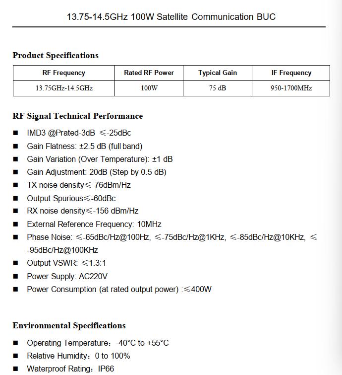
- Production consistency comes from closed-loop calibration, not from component tolerance. Five controls cover device dispersion, process, and assembly variation.
This is a practical walkthrough of taking a self-organizing mesh video datalink from a requirements document to volume delivery. The target is a typical L/S-band unit: 20 km line-of-sight range, end-to-end latency under 40 ms, AES-128 encryption, a single 12 V supply, 33 dBm transmit power, adaptive QPSK/16QAM/64QAM modulation, two 100 Mbps Ethernet ports, SMA-K RF connectors, and an operating range of -20 to +60 degrees C. The numbers look modest. Making them all true at once, and keeping them true across a thousand units, is where the difficulty lives.
Before We Start: Three Red Lines
Three rules frame everything that follows.
Compliance first. RF products are not ordinary consumer goods – what they radiate is regulated. Transmit power, spurious emissions, occupied bandwidth, and out-of-band rejection must each be checked against the applicable national frequency allocation rules and the certification requirements for the product category. Do not try to buy range by simply cranking up the power amplifier. The goal is to extract distance inside the legal power budget through link budget discipline, antenna gain, low noise figure, and an efficient power amplifier.
Domestic sourcing. For this project the requirement is hard: the core FPGA, power amplifier MMIC, RF switches, LNA, mixers, PLL, filters, and the key capacitors, inductors, resistors, crystals, connectors, and mechanical parts all come from domestic suppliers. Each device category below includes the brands and part families actually in use, along with the pitfalls encountered when substituting them.
Manufacturability. Getting one prototype running on the bench and shipping a thousand units reliably are two entirely different worlds. The final chapter covers production: how to control consistency, how to localize and eliminate batch-level specification drift, and how to run burn-in screening.
One caveat about every part number mentioned: they are devices actually used, or currently running on production lines, and the recommendations reflect practical experience. But device selection is never a matter of copying a part number. Different batches of the same part, drifting peripheral parameters, and dielectric constant variation between board houses will all move your measured performance. Always confirm against the manufacturer’s latest datasheet and re-verify against your own product’s specifications.
A Necessary Caveat: On Satellite Interference
There is work in the industry on so-called satellite constellation jamming and, more broadly, on anti-satellite RF equipment. That needs to be stated plainly, both for the reader’s benefit and for compliance reasons.
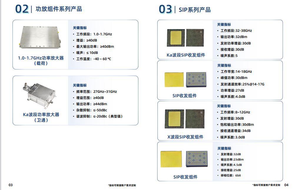
The legitimate product categories here are compliant radio equipment with clearly defined lawful uses: RF microwave front ends and wideband power amplifiers for counter-drone jamming and detection systems, self-organizing mesh communication datalinks, radio monitoring and spectrum management equipment, and compliant radio test and electronic countermeasures training equipment. All of these require clearly defined lawful use and the appropriate approval and licensing processes.
Where this article mentions counter-drone systems, RF microwave components, wideband power amplifiers, or spaceborne applications, it is discussing amplifier design, link budgets, electromagnetic compatibility, and transmit-receive isolation in a purely engineering context. It does not provide, and does not discuss, any specific operational method for interfering with a particular civilian satellite constellation. That would be neither compliant nor within a professional engineer’s ethical scope. Technology is neutral; its application has boundaries, and engineers need to hold the line.
What is genuinely worth a career of study are the hard problems that create value inside the compliance framework: wideband transmit and receive front ends for counter-drone radar, high-power high-efficiency amplifiers, high dynamic range receive chains, multi-channel T/R modules, and millimeter-wave RF front ends. Those directions are deep enough, hard enough, and durable enough to sustain an entire engineering career.
Chapter 1: Requirements Assessment
1.1 The First Step After Receiving the Requirements Document
The most common mistake is to skim the specifications and immediately open a schematic tool. That leads to repeated rework and a stalled project. The correct first step is to sit down, translate every specification into a concrete engineering constraint, and do the arithmetic – link budget, power, thermal, cost, and compliance. If those five sets of numbers are not settled, everything downstream is built on air.
No one on the team touches a schematic tool during the first week of a new project. The only deliverables are a requirements breakdown table and a link budget table. Both go into the project file and become the basis for every subsequent design review.
1.2 Link Budget: Where the 20 km Figure Comes From
Range is extremely sensitive to link loss. A few dB of difference is a multiple in distance, so the arithmetic matters.
The free-space path loss formula is: Lfs = 32.44 + 20log10(f) + 20log10(d), where f is in MHz and d is in kilometers. At a center frequency of 1400 MHz (L-band; the actual allocation depends on the project and radio regulations, this is an example calculation), the free-space path loss at 20 km is: 32.44 + 20log10(1400) + 20log10(20) = 32.44 + 62.9 + 26.0, approximately 121.4 dB.
That is a sobering number. Power transmitted is down 121 dB by the time it reaches the receiver at 20 km.
A typical breakdown: 33 dBm transmit power, 2 dB transmit antenna gain (a realistic figure for a portable unit), 2 dB receive antenna gain, and a receiver sensitivity on the order of -105 dBm for a 10 MHz bandwidth at a 6 dB SNR requirement. Total received level: 33 + 2 + 2 – 121.4 = -84.4 dBm. Against -105 dBm sensitivity, that leaves 20.6 dB of margin.
That 20.6 dB is the entire safety cushion, and it disappears quickly. Antenna misalignment costs 3 to 5 dB. Feed line loss costs 1 to 2 dB. Multipath fading and tree blockage cost 5 to 10 dB. Transmitter power droop with temperature costs 2 to 3 dB. VSWR mismatch return loss costs 1 to 2 dB. Added up, more than ten dB is gone. That is why the transmit power must reliably exceed 33 dBm and why the power amplifier needs temperature and voltage compensation – margin is nibbled away in the worst case, so the design has to carry enough of it.
The link budget table should never be computed at room temperature and nominal values only. It needs at least three columns: nominal, temperature extremes, and worst-case combination (high temperature plus low voltage plus antenna mismatch simultaneously). The production design goal is for the worst-case column to still meet margin. A design validated only at nominal values will fail in production.
1.3 The 40 ms Latency Budget
Forty milliseconds is a system-level hard constraint for a mesh datalink, and the RF chain contributes a meaningful share.
The main contributors: baseband and FPGA processing delay, which is controllable and should be optimized to a few milliseconds; local oscillator lock time, where a PLL takes anywhere from hundreds of microseconds to several milliseconds to lock, and fractional-N PLLs deserve extra attention because lock time is directly set by loop bandwidth; transceiver filtering and digital up/down conversion delay, typically a fraction of a millisecond to a few milliseconds; power amplifier switching response, generally microseconds and negligible, though saturation recovery time matters; and multipath-induced inter-symbol interference at the antenna, which is environment-determined and can only be absorbed through equalization and coding.
Added together, the intrinsic RF and baseband delay should stay within about 10 ms, leaving 30 ms for the protocol stack, network layer, and application layer queuing and retransmission. One trap worth flagging: if the power amplifier is designed too aggressively for efficiency at high power and runs deep into saturation, then the moment amplitude control or burst transmission is required, the switching transient trails off – and that tail eats directly into the latency budget while degrading adjacent channel leakage ratio (ACLR). Latency cannot be assessed module by module; it has to be assessed end to end.
1.4 Translating Every Specification Into a Circuit Constraint
Transmit power, 33 dBm. That is 2 W. In a handheld device that is substantial; in a vehicle-mounted unit it is moderate. At this power level, thermal management, supply, linearity, and harmonic suppression all matter without exception.
Operating band. A compliant sub-band within L/S band, with the exact frequency set by the project approval document. This band has a high degree of domestic device availability and a wide selection, making it the best value choice.
Adaptive QPSK / 16QAM / 64QAM. This is a critical point. Different modulation orders place very different demands on amplifier linearity. QPSK tolerates deeper back-off, so efficiency can be relatively high. 64QAM has extremely tight error vector magnitude requirements, forcing the amplifier into a much more linear region with more back-off and sacrificed efficiency. The amplifier design must therefore support dynamic bias control – automatically raising bias current to preserve linearity at high modulation orders and lowering it for efficiency at low orders.
Latency, 40 ms. Covered above; a system-level constraint.
AES-128 encryption. Baseband and FPGA territory. The RF side does not manage it, but sufficient data throughput bandwidth and clock resources must be reserved.
Single 12 V DC supply. This is a cost driver and a design difficulty. With 2 W of RF output and a power amplifier efficiency of 30 percent (broadband amplifiers struggle to exceed 40 percent), the PA stage alone draws 6.7 W. Add baseband, FPGA, LNA, and PLL, and total consumption moves toward 12 W – which is 1 A at 12 V. Power paths, decoupling, and PCB copper widths all have to be designed for that current.
Operating temperature, -20 to +60 degrees C. A typical industrial and defense envelope, not comparable to consumer parts rated to +70 degrees C junction. Every critical device must be checked across the full temperature range, especially power amplifier gain drift, crystal frequency drift, and inductor and capacitor temperature coefficients – these three drive most full-temperature degradation.
Interfaces. Two 100 Mbps Ethernet ports and two SMA-K RF connectors. Interface choices determine the mechanical layout and EMC protection design.
Size and weight. Portable equipment is extremely weight-sensitive. Heat sinks, shielding covers, and connectors are all weight and must be accounted for carefully.
1.5 System Architecture
The classic architecture works best here: RF transceiver plus FPGA plus wideband power amplifier plus LNA plus local oscillator chain. It is the most mature, the most controllable, and the easiest to manufacture.
Transmit path: the FPGA generates baseband I/Q data and hands it to the transceiver for digital upconversion and DAC, producing a zero-IF or low-IF signal; RF filtering and a variable gain amplifier provide pre-amplification and out-of-band rejection; a wideband PA drives it to 33 dBm; a directional coupler samples forward and reflected power for the detector-based power monitor; the signal exits through an antenna switch or circulator to the SMA-K port.
Receive path: the signal enters through the antenna port and passes an antenna switch, limiter, and LNA to amplify the weak signal; filters and a mixer downconvert to IF, or the signal goes directly into the transceiver receive channel for ADC and digital downconversion; the digital stream goes to the FPGA for demodulation, equalization, decoding, and networking protocol processing.
Local oscillator chain: a highly integrated frequency synthesizer (PLL plus VCO, or an external VCO with a PLL) generates the LO, split by a power divider to the transmit upconverter and the receive mixer. LO phase noise directly sets the receiver’s adjacent channel selectivity – a point many people overlook.
Power chain: 12 V input goes through DC-DC converters to produce the rails – 5 V for PA bias and control, 3.3 V and 1.8 V for FPGA and transceiver I/O, 1.2 V or 0.9 V for the FPGA core. Each rail needs its own pi filter and adequate decoupling.
Monitoring chain: the FPGA samples temperature, voltage, current, forward power, reflected power, and VSWR through ADCs for closed-loop control. In a production product this chain matters a hundred times more than it does on a prototype, because it determines whether you can automatically compensate device dispersion at volume.
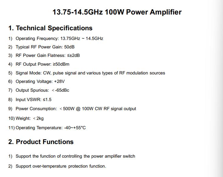
The architecture looks like a textbook exercise, and that is exactly the point. Production products want this kind of unglamorous maturity. Every flashy innovation gets ground down by cost and reliability during prototyping. The real skill is understanding and nailing every parameter of a mature architecture.
1.6 Device Selection, Part 1: FPGA, RF Transceiver, PLL and VCO
1.6.1 FPGA: The System’s Center
The FPGA handles baseband processing, the protocol stack, interface control, and the ADC/DAC interfaces. Domestic FPGAs have improved quickly and are already running on multiple production models.
Domestic FPGA vendors fall into three tiers. The first tier is Anlogic (Shanghai), whose EG4 and ELF2 families offer excellent value, with logic densities from a few thousand to over a hundred thousand equivalent logic cells, built-in hard ARM cores or soft RISC-V cores, on-chip PLLs and global clock networks, and the TangDynasty (TD) toolchain that is quick to learn. For this project a mid-range Anlogic device with 50,000 to 150,000 equivalent logic cells is appropriate, at roughly 30 to 50 percent of the price of an equivalent imported part.
The second tier is Gowin Semiconductor (Guangdong), whose LittleBee and GW2A families are very competitive in cost-sensitive designs, with the Gowin EDA toolchain. If cost is the dominant constraint and logic demand is modest, Gowin is the first choice. The third tier is Pango Micro, whose Logos and Titan families target the mid-to-high end with larger logic capacity and stronger high-speed interface capability, suited to designs needing DDR3 or high-speed SerDes. Pricing is higher, but the domestic substitution maturity is high.
Key selection criteria, all learned the hard way. Resource headroom: post-synthesis logic utilization should stay under 70 percent, Block RAM under 80 percent, and PLL usage under two thirds. The protocol stack will change and features will be added; no headroom means disaster later. Clock resources: RF systems are demanding about clock quality, so check how many global clock buffers and PLLs the device offers and whether they can supply multiple same-source clocks. Configuration device: the SPI flash configuration memory should also be domestic, for example SPI NOR from Fudan Microelectronics or Dosilicon. Toolchain version: lock it down. A tool upgrade can change timing constraints and place-and-route results, and production code must never drift with toolchain upgrades.
The most common pitfalls when replacing an imported FPGA such as a Xilinx Artix-7 or Zynq-7000: pin compatibility, since domestic packages usually differ and the layout must be redone rather than dropped in; primitive and IP core incompatibility, especially DSP blocks, Block RAM, and clock management primitives, which must be re-instantiated; timing closure, which sometimes requires code optimization to hit the same frequency on a domestic process; and simulation libraries, which must be recompiled for ModelSim or Verilator. Each of these can cost a month of schedule.
1.6.2 RF Transceiver: Integrated or Discrete
Option A is a highly integrated zero-IF transceiver that contains the DAC, ADC, digital up and down conversion, quadrature modulator and demodulator, programmable gain amplifiers, and a fractional-N local oscillator in one die. The advantages are a short bill of materials, good consistency, simple bring-up, small footprint, and low power – ideal for volume production. The disadvantage is inflexibility: bandwidth, gain, and filter characteristics are fixed by the chip.
Option B is discrete: separate I/Q modulator and demodulator with external DAC/ADC and an external local oscillator. The advantages are wide achievable bandwidth, customizable specifications, and rich debugging options. The disadvantages are a longer bill of materials, I/Q quadrature error that must be calibrated, DC offset that must be handled, and consistency that depends on tuning.
For a mesh datalink with bandwidth inside a few tens of MHz and high volume, the integrated transceiver wins decisively on manufacturability. Discrete designs are for bandwidth beyond roughly 100 MHz or for high-end models with special in-band spurious requirements. Do not choose discrete just because it sounds more sophisticated.
Selection criteria: leave 2x margin on bandwidth rather than using it right to the edge; close-in phase noise (at 1 kHz offset) directly affects receive sensitivity and should be better than -100 dBc/Hz; LO lock time should be in the microsecond to millisecond range or the burst communication latency target will not be met; transmit-receive isolation inside the chip must be adequate or the receiver can be blocked by its own transmit leakage; and the reference clock should come from a domestic TCXO or OCXO with stability better than plus or minus 0.5 ppm.
1.6.3 PLL and VCO: The Soul of the LO Chain
Domestic PLL options include the JMF family from Beijing Shidai Minxin (part of the 772nd Institute under China Aerospace Science and Technology Corporation), which offers stable performance and aerospace-grade screening options; the PLL line from Chengdu Huawei Microelectronics; and frequency synthesizers from CETC Institute 24. For cost-sensitive designs, some PLL products from Beijing Zhaoxun Hengda and Shanghai Belling are also usable.
PLLs with integrated VCO offer high integration and a simple peripheral network, which suits volume production. Domestic vendors include Nanjing Zhongkewei and Shenzhen Ruineng Micro; the specific part depends on the target band. Where wider frequency coverage or lower phase noise is needed, an external VCO is required. Domestic VCO vendors include Wuhan Fingu and Tatfook, plus the VCO families from CETC Institute 13. Three VCO parameters matter: tuning sensitivity (Kvco, in MHz per volt) must not be too high, or supply noise modulates directly onto the carrier as phase noise; phase noise must meet the system requirement; and output power must match the input level of the following divider and mixer.
The passive components around the LO chain look trivial but are a hidden killer of production consistency. The loop filter resistors and capacitors should be thin-film resistors at 1 percent tolerance and C0G/NP0 capacitors at 5 percent. Loop bandwidth sets both lock time and close-in phase noise, and loop bandwidth is determined by those RC values. Using ordinary thick-film resistors at 5 percent and ordinary X7R capacitors at 20 percent with a strong voltage coefficient means the actual loop bandwidth can differ from the calculated value by a factor of two – and in production some boards lock in a second while others take ten. That is an extremely painful problem to debug. Loop filter components are not the place to save money.
1.7 Device Selection, Part 2: PA, LNA, Switches, Mixers, Attenuators
1.7.1 The Power Amplifier
There are three approaches, in order of recommendation.
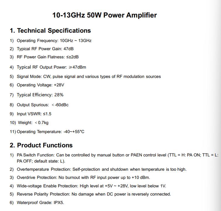
First: domestic PA MMICs. This is the preferred and most recommended volume approach. Domestic RF PA MMIC vendors are mature. Commonly used families include CETC Institute 13’s GaAs power MMICs covering L to C band with output from a few hundred milliwatts to several watts, and CETC Institute 55’s GaN MMICs, where GaN offers better power density, voltage withstand, and thermal stability for high-power scenarios. On the commercial side, Chengdu Jianahaiwei, Nanjing Guobo Electronics, Suzhou Innoscience, and Xiamen Sanan Integrated Circuit all have reasonably complete RF power MMIC lines.
For this 2 W, L/S-band case, a two-stage cascade is appropriate: a gain block or driver amplifier MMIC providing 15 to 20 dB of gain, followed by an output-stage power MMIC delivering 2 to 3 W (33 to 35 dBm). An attenuator or isolator between the stages handles inter-stage matching and isolation. Total gain lands at 30 to 35 dB, so an input drive of -5 to 0 dBm is enough to reach full output – which matches the transceiver’s output level.
When selecting the output stage, do not look only at saturated output power. Check the datasheet’s linear output power and ACLR under the modulation scheme you will actually use. That is the real specification.
Second: discrete FET or HEMT designs. Using domestic GaN HEMT or LDMOS devices with a custom matching network. Domestic device vendors include Suzhou Innoscience and Dalian Xinguan for GaN HEMTs, and CETC Institute 55 for GaN devices. The advantage is higher efficiency (above 50 percent) and higher power; the disadvantages are design difficulty, consistency that depends on tuning, and high production tuning cost. Discrete designs make sense mainly for ultra-wideband, high-power scenarios above 10 W. For a 2 W portable product, the MMIC approach wins decisively.
Third: hybrid modules. Many domestic vendors supply packaged amplifier modules that work out of the box. The advantages are convenience and good consistency; the disadvantages are cost, size, and poor customization. They are fine for early validation or small batches, but volume production should integrate MMICs directly, which can halve the cost.
The most critical selection criteria: large-signal load-pull data, which must come from the vendor or from your own load-pull measurement. Designing matching from small-signal S-parameters alone is a classic beginner mistake, because the optimum load impedance under large-signal drive is nothing like what small-signal S-parameters imply. Also check the trade-off between saturated output power and linearity, which sets your back-off; power added efficiency across temperature, which drives thermal and endurance design; the gain compression curve and its 1 dB compression point drift with temperature, which decides whether full-temperature specifications pass; input and output VSWR, which affects matching and reflected power; harmonic output levels, which determine EMC and certification; and ESD and latch-up protection, since GaN devices are extremely static-sensitive.
1.7.2 LNA, Switches, Mixers, Digital Step Attenuators
RF switches for transmit-receive switching: GaAs switch MMICs are the usual choice. Selection criteria are insertion loss (under 1 dB), isolation (above 30 dB), power handling (must withstand the 33 dBm transmit leakage), and switching time (microseconds). One warning: the power handling rating should carry 2x margin over maximum transmit power, because antenna mismatch sends reflected power back into the switch, which is the device most likely to be destroyed.
Mixers, needed if a superheterodyne architecture is used: diode mixer MMICs or Gilbert cell active mixer MMICs from CETC Institute 13 are typical. Selection criteria are conversion loss or gain, port isolation (LO leakage, RF leakage), and third-order intercept point.
Digital step attenuators for fine transmit power adjustment and automatic gain control: GaAs digital step attenuator MMICs. Selection criteria are attenuation step (0.5 or 1 dB), attenuation range (31.5 dB is common), insertion loss, and attenuation accuracy.
1.8 Device Selection, Part 3: The Critical Passives
Domestic passives vendors in the first tier include Guangdong Fenghua Advanced Technology, Fujian Torch Electron Technology, Beijing Yuanliu Hongyuan, and Shenzhen Eyang. Several hard rules apply to RF use.
First, capacitors in RF bypass and matching networks must be C0G/NP0 dielectric, never X7R or X5R. C0G has a temperature coefficient near zero (plus or minus 30 ppm per degree C) and no DC bias effect – capacitance does not shift with operating voltage. An X7R capacitor under 12 V bias can lose half its nominal value, which completely changes your impedance in a matching network.
Second, decoupling capacitors should be paralleled in layers: 10 microfarads of tantalum or ceramic for low-frequency energy storage, then 1 microfarad, 0.1 microfarad, 0.01 microfarad, and 1000 picofarads in parallel, covering the decoupling band from low to high frequency. Each level goes as close to the device power pin as possible.
Third, RF bypass capacitors need ground vias taking the far terminal to the ground plane as directly as possible. Via inductance eats high-frequency decoupling performance, so high-power devices need at least two vias per ground pin and critical nodes need four or more.
1.9 Second Sources and Substitution Rules
Principles for establishing a second source: electrical parameters must be compatible across voltage, current, frequency, power, and interface levels; the package should be compatible with as close to identical pinout as possible, and at minimum requires an adapter board evaluation; RF performance must be benchmarked by measuring S-parameters on a VNA and output power and spurious on a spectrum analyzer, never from the datasheet alone; reliability must be benchmarked through temperature, vibration, and aging comparison tests; and the supply chain must be confirmed by establishing direct contact with both vendors and obtaining formal price and lead-time commitments.
The substitution process belongs in the design specification: any device change must pass through four stages – engineering change notification, laboratory verification, small-batch pilot production, and volume release – each with data and approval records. The process looks cumbersome, but it saves projects. Many projects have been sent back for full rework because a component quietly changed batch and the whole production run drifted.
Chapter 2: Schematic Design
2.1 A Schematic Is Not Wiring – It Is Engineering Discipline
Hierarchical organization: split the design by function into pages – cover and revision page, power tree, FPGA and configuration, baseband interfaces, RF transceiver, PA chain, receive chain, LO chain, monitoring and interfaces, and connector breakouts. Each page carries its name and revision at the top, so anyone picking up the drawing can navigate quickly.
Readability: signal flow always runs left to right, power flow top to bottom. Every device needs a complete designator and part number. Every critical net needs a net name. Bypass capacitors, pull-up and pull-down resistors, and configuration resistors must never be omitted – they are the foundation of production consistency.
Traceability: every device’s package, designator, part number, and parameters must be findable in the bill of materials. Every pin’s function, voltage, and current must be verifiable in the datasheet. During schematic review, walk every page against the datasheet pin definitions rather than assuming.
2.2 Power Tree Design
The architecture: 12 V first goes through a synchronous buck converter to 5 V, which must deliver more than 3 A at better than 90 percent efficiency for the PA bias, RF switches, and mixers. That 5 V rail then goes through another buck to 3.3 V for the FPGA I/O, transceiver, and clock circuits. The 3.3 V rail goes through a low dropout regulator to 1.8 V, and then through an ultra-low-noise LDO to 1.2 V or 0.9 V for the FPGA core.
Why an LDO for the core? The FPGA core draws large, rapidly changing current, and a switching supply’s transient response cannot keep up, which causes logic errors and power integrity problems. The LDO is lossier but delivers clean power.
One production lesson worth emphasizing: every critical node in the power tree should have a reserved test point, labeled with its voltage and tolerance – for example “5V plus or minus 5 percent.” These test points are lifesavers during production bring-up. A new engineer with a multimeter can confirm each rail step by step instead of immediately suspecting the chips.
2.3 RF Transceiver Interface Circuits: I/Q, Clock, Configuration
I/Q data interface: an LVDS serial interface at a few hundred megabits per second, routed as differential pairs with 100 ohm differential impedance control. Clock interface: the transceiver reference clock should come from a dedicated clock chip or crystal, routed short and away from noise sources, with 33 ohm series matching resistors on both sides. Configuration interface: the SPI bus typically runs at 10 to 50 Mbps and needs 0.1 microfarad decoupling and 1 kilohm pull-ups.
2.4 The PA Chain Schematic
This is the core of the schematic, and the matching network is where the design is won or lost.
2.5 Wideband RF Matching: The Technical Core
2.5.1 The Nature of Matching: Conjugate vs Power Matching
The workflow for a power amplifier matching network: first, use a load-pull system to find, across the target band, the intersection region of the equal-power, equal-efficiency, and equal-linearity contours that satisfies the output power, efficiency, and linearity requirements, and identify an optimum load impedance (usually complex). Second, transform that optimum load impedance to the 50 ohm system impedance with an impedance transformation network. Third, synthesize the matching network on a Smith chart. Fourth, optimize with electromagnetic simulation. Fifth, fabricate and fine-tune on the bench.
Why is wideband harder? Narrowband matching only has to be correct at a single frequency point. Wideband matching must hold across the entire operating band – for example 1.2 to 1.6 GHz, nearly 30 percent relative bandwidth – which demands a flat frequency response from the transformation network. Narrowband can use high-Q LC networks for sharp matching; wideband requires reactance compensation, tapered transmission lines, and multi-section transformers.
2.5.2 Eight Common Matching Topologies
1. L-match. One series reactance and one shunt reactance, shaped like the letter L. The series arm transforms the real part while the shunt arm cancels the imaginary part. Advantages: few components, low loss, moderate bandwidth. Disadvantage: only one transformation ratio and a relatively high Q, which limits bandwidth. This is the most frequently used topology and deserves thorough understanding. If the series arm is an inductor it is a low-pass L-match; if it is a capacitor it is a high-pass L-match. The low-pass form also suppresses harmonics, which is why it is more common in power amplifiers.
2. Pi-match. Shunt reactances at both ends with a series reactance in the middle. It can achieve very large transformation ratios – for example a few ohms to 50 ohms – with good input-to-output isolation. But Q is high, bandwidth is narrow, and component values are frequency-sensitive. Used for output matching of the final stage and antenna port matching. If the middle series arm is an inductor, it must be chosen with a self-resonant frequency well above the operating band.
3. T-match. The dual of the pi-match: series reactances at both ends with a shunt reactance in the middle. It also achieves large transformation ratios, but with the series elements on the low-impedance side and the shunt element on the high-impedance side. Used for input matching, where many power amplifiers present a low input impedance in the 5 to 10 ohm range, and for source or drain matching.
4. Baluns and differential matching. Many transceivers, mixers, and power MMICs have differential interfaces, so an LC or transformer balun is needed to convert single-ended 50 ohms to a differential impedance. Selection criteria are operating band, insertion loss (under 1 dB), and amplitude and phase balance (better than 0.5 dB and 5 degrees).
5. Transmission line matching. At higher frequencies (C band and above) or higher power, lumped elements lack sufficient Q, self-resonance margin, and power handling, so microstrip does the matching. Common forms are the quarter-wave transformer – a quarter-wavelength line of characteristic impedance equal to the square root of Z1 times Z2 placed between Z1 and Z2 – multi-section quarter-wave transformers for broadband work with Chebyshev or binomial responses, and tapered lines for ultra-wideband use. Trace width is set by the board dielectric constant, thickness, and copper weight, so use an impedance calculator and surround the traces with a via fence for shielding.
6. Klopfenstein taper. The go-to for ultra-wideband matching. It delivers smooth impedance transformation across a very wide frequency range with an extremely flat response. The cost is board area. Used for octave and wider power amplifiers and ultra-wideband transmit and receive front ends.
7. Lumped-element low-pass filter matching. Combining the matching network and the filter into one, a common power amplifier technique. A seventh-order Chebyshev low-pass topology can perform impedance transformation and harmonic suppression simultaneously. Electromagnetic simulation is mandatory.
8. Active matching and predistortion. A high-end approach. A predistortion network, analog or digital, is placed ahead of the amplifier so the input signal acquires a nonlinearity inverse to the amplifier’s, cancelling it and improving linearity. Rarely used in volume products, but worth knowing as a direction.
2.5.3 Key Matching Specifications
VSWR and return loss. Input VSWR below 1.5 (return loss better than 14 dB) and output VSWR below 2 (return loss better than 10 dB). Poor VSWR means high reflected power, low efficiency, severe heating, and in extreme cases destruction.
In-band gain flatness. Gain variation across the operating band under plus or minus 0.5 dB, and at worst under plus or minus 1 dB. Flatness is controlled by the matching network frequency response and must be checked frequency point by frequency point.
Insertion loss. The matching network itself has loss, and in wideband designs with low-Q components it is not negligible. Total insertion loss should stay under 0.5 dB, since it feeds directly into efficiency.
Harmonic rejection. Second and third harmonics must be suppressed by the matching network and output filter to below -40 dBc and -30 dBc respectively. This affects certification and EMC.
Large-signal stability. The amplifier must be unconditionally stable under large-signal drive with no self-oscillation. Perform stability circle and mu-factor analysis, requiring mu greater than 1 and the determinant magnitude below 1. Self-oscillation is the most common disaster in power amplifier design, especially in wideband designs, where the low band (tens to hundreds of MHz) and high-end multiples oscillate most readily. Remedies include neutralization capacitors, negative feedback resistors, and better ground vias in the bias network.
2.5.4 Matching Network Tuning in Practice
Step one, small-signal tuning. With no power applied, bias the amplifier into its linear region (class AB or class A) and measure S-parameters on the VNA. Tune the input matching network until S11 is below -10 dB across the band, and the output network until S22 is likewise below -10 dB. Remember this is only small-signal matching.
Step two, large-signal tuning. Using a signal source and power meter, increase input power gradually to find the 1 dB compression point and saturated power. Then use a load-pull system, varying the output load impedance through a tunable matching network or mechanical tuner, to observe output power, efficiency, and linearity and identify the optimum impedance. Fix that transformation network on the PCB.
Step three, harmonic tuning. Under saturation the optimum load differs for the fundamental, second, and third harmonics. Adding a network that shorts the second harmonic while presenting the optimum load at the fundamental significantly improves efficiency and output power. This is a dividing line between experienced and inexperienced designers.
Step four, full-temperature re-test. Re-measure S-parameters and power at -20 and +60 degrees C and record the drift. If drift is excessive, introduce temperature compensation into the matching network, such as a temperature-compensating diode or NTC thermistor in the bias circuit that adjusts bias automatically with temperature.
Step five, freeze the parameters. Commit the tuned matching component values to version control, then fabricate a second PCB revision to verify repeatability – at minimum five boards and ten chips spanning different batches – and confirm the specification distribution. If your numbers are only met on one board with one chip, that is not a design, it is luck.
2.6 Receive Chain and LNA Matching
LNA matching splits into two parts: the input is matched for noise, minimizing the noise figure, while the output is conjugately matched to transform the LNA’s typically high output impedance to 50 ohms. The same L, pi, and T topologies apply, with component values balancing noise figure against gain. Tune with a noise figure analyzer to measure noise figure directly while using the VNA to check gain and VSWR.
2.7 LO Chain and PLL Loop Filter Design
Loop bandwidth is the core PLL parameter. Inside the loop bandwidth, phase noise is dominated by the reference clock and phase detector noise; outside it, phase noise is set by the VCO. A wide loop bandwidth gives fast lock and good close-in phase noise tracking the reference, but lets close-in spurious through. A narrow loop bandwidth locks slowly with poorer close-in phase noise tracking the VCO, but suppresses spurious well. This trade-off must be made deliberately.
For a burst communication system requiring millisecond lock times, the loop bandwidth should be relatively wide, typically in the tens of kilohertz. A third-order passive loop filter is used to suppress phase detector spurious. The standard topology uses two series resistors controlling the zeros, two shunt capacitors controlling the poles, and an R3C3 high-frequency filter. Values should be computed with a PLL simulation tool and then realized with 1 percent thin-film resistors and 5 percent C0G capacitors.
The VCO tuning port is a high-impedance, highly sensitive node that must be well filtered and shielded. Add an RC low-pass filter on the tuning line – for example 1 kilohm and 1000 picofarads – and route it away from digital and power lines so digital noise cannot modulate onto the carrier as phase noise.
Chapter 3: RF PCB Design
3.1 The PCB Is the Second Half of the Design
When the schematic is done, only half the design exists. The other half is on the PCB. The ideal wire in a schematic becomes a trace with length, width, impedance, and crosstalk on the board. The copper between two capacitors is an inductor; a trace and the ground beside it form a capacitor. Every parasitic in an RF design is drawn into the PCB.
The governing principles are five: layering, partitioning, grounding, impedance, and symmetry.
3.2 Stackup Design
A six-layer board is recommended. From top to bottom: top layer (RF and components), layer two (solid ground plane), layer three (inner RF signals and critical routing), layer four (power plane), layer five (ground), and bottom layer (low-speed signals and test points).
Why six? The power amplifier needs a solid reference ground for return currents and enough isolation to separate the PA output, a strong signal, from the LNA and local oscillator, which are weak. Four layers cannot achieve that isolation and eight layers cost too much. Six is the best value.
Material choice is critical. Standard FR-4 has a dielectric constant of 4.2 to 4.5, but it varies with frequency and temperature, varies between batches, and has a high loss tangent around 0.02, which becomes noticeable above 1.5 GHz. Use a high-frequency material for the RF layers. Domestic options include Shengyi S7136H and S7439, or a PTFE composite such as Rogers 4350B with domestic equivalents. Mixed lamination – high-frequency material 0.2 to 0.3 mm thick for RF signal layers and standard FR-4 for the rest – increases fabrication cost but the RF performance improvement justifies it.
Copper weight: 1 oz (35 micrometers) on the outer layers and 0.5 oz inner. High-current PA traces should be locally thickened to 2 oz or opened for solder. Dielectric thickness must be controlled precisely with an impedance calculator, targeting 50 ohm characteristic impedance within plus or minus 10 percent.
3.3 Partitioned Layout
The first layout action is partitioning. Divide the board into territories: the PA area (strong signals, the most dangerous), the receive chain (LNA and mixers, the most sensitive), the LO area (PLL and VCO, highly sensitive), the digital area (FPGA and power, a noise source), and the power area.
The iron rule: the trace from the PA output to the antenna port must never pass through the LNA, the LO, or any part of the receive chain. That trace is the strongest radiator on the board; once it couples into the receive chain, sensitivity drops at best and at worst the receiver is blocked by its own transmit leakage and the unit is dead. Place the PA at the board edge near the antenna connector and the LNA and LO at the far end, separated by a grounded shielding wall.
Shielding cans are standard in production products. The RF area, LO area, and receive area should all have metal shields. The shield ground must connect to a solid ground plane through dense via stitching – spacing under one tenth of a wavelength, which is under 2 cm at 1.5 GHz – forming a Faraday cage. Absorber material inside the shield further suppresses cavity resonance.
3.4 RF Routing Rules
Continuous impedance. All RF traces are 50 ohm microstrip with widths calculated precisely. Any change in width, spacing, or reference plane distance creates an impedance discontinuity and a reflection. Corners must use arcs or two 45-degree segments, never a 90-degree right angle, whose equivalent capacitance causes an impedance dip.
Shortest path. RF traces should be as short as possible. This matters most in the PA input and output matching networks, where a few millimeters of copper between components can be several nanohenries of parasitic inductance – enough to throw the match completely off. Matching components must sit tight against the amplifier pins with no vias or long runs in between.
No plane splits. The reference ground plane under an RF trace must be solid, with no crossing between different ground planes such as the gap between digital and analog ground. Crossing a split lengthens the return path and produces severe radiation and crosstalk.
Ground via arrays. Every RF device ground pin needs at least two ground vias nearby, and critical devices such as the PA, LNA, and mixers need four or more. Via inductance must be low, so use larger diameters (0.3 mm and up) and more of them. Surround the RF area with a via fence at spacing under one twentieth of a wavelength.
Matched differential pairs. I/Q and clock differential pairs must be length-matched within 100 mil (2.5 mm), spacing-matched, tightly coupled, and symmetrically via’d.
Avoid long parallel runs. Two RF traces running parallel over distance will couple. When parallel routing is unavoidable, keep spacing above three trace widths.
3.5 Power and Ground on the PCB
Power routing carries low-frequency, high current, but it is the main noise source and, handled badly, contaminates the whole RF system.
Power paths must be wide. The 12 V input and the 5 V and 3.3 V main runs should use copper pours at least 50 mil (1.27 mm) wide, with high-current paths such as PA supply at 100 mil or more, or a full pour. Connect pours to the inner power plane through multiple vias to lower loop impedance.
Ground planes must be solid. Layers two and five must be fully poured and not cut up by signal traces. All ground vias, device grounds, and connector grounds terminate on these planes. Analog and digital ground should be single-point connected, usually at the power entry point through a ferrite bead or directly, depending on system noise. In an RF system, do not split ground unless you must – a badly handled split creates an antenna. Single-point grounding is the safer choice.
Decoupling capacitor placement is a discipline of its own. Every power pin’s decoupling capacitor goes tight against the pin with the shortest possible return to ground. The 0.1 microfarad part goes closest, the 10 microfarad part can be slightly further. Capacitor ground pads need at least two ground vias. This sounds simple, but many boards suffer power integrity problems, amplifier self-oscillation, and FPGA timing errors purely because decoupling capacitors were placed too far away.
3.6 Mechanical and Thermal Coordination
The PCB is not isolated – it mounts into an enclosure and onto a heat sink, so layout and mechanical design must proceed together.
Thermal vias: power MMICs and power devices need via arrays on their thermal pads – for example a grid of 0.3 mm vias at 1 mm pitch – conducting heat to the inner ground plane and the back-side copper, then to the chassis. Vias should be copper-filled or tented to prevent solder wicking during reflow.
Mounting holes: reserve mounting holes around the board edge with positions matching the chassis, and add keep-outs so screwdrivers cannot short anything.
Connector and mechanical alignment: the SMA-K connector position and orientation must match the panel cutouts to within 0.1 mm, or the unit will not fit or will make poor contact. Bring the mechanical 3D model into the layout and check the overlay.
Board thickness and tolerance: weight- and volume-sensitive products should keep board thickness at or under 1.6 mm, with 1.2 mm recommended. Board thickness affects microstrip impedance, so once material and thickness are fixed they cannot be changed casually – any change means recalculating every match.
3.7 DFM and DFT
Production design must respect the process capability of the board house and the assembly house.
Trace width and spacing: standard processes handle 4 mil/4 mil, but RF microstrip typically needs 6 to 10 mil. Do not design to the process limit; leave 20 percent margin. Via sizes: standard 0.3 mm drill with 0.6 mm pad; laser microvias can reach 0.1 mm but cost more. Standard vias are sufficient here. Solder mask: keep solder mask dams between closely spaced pins such as FPGA BGAs and fine-pitch PA MMIC leads to prevent bridging. Silkscreen: every reference designator, polarity, and orientation must be clearly marked. Test points: production boards must reserve adequate test points – key power nodes, coupling and sampling points at critical RF nodes, clocks, configuration signals, power detection, and temperature sensing. Every critical node must be probeable with a single tip, and every RF stage must allow breaking the chain to inject a test signal. Panelization: account for V-cut or mouse-bite positions so depaneling does not damage edge components.
3.8 Pre-Fabrication Checklist
Eight checks before releasing the board, which typically save at least two rounds of rework.
One, schematic review: is each device’s supply voltage correct? Is any pin floating? Are configuration pin levels correct? Are pull-ups and pull-downs present? Are any decoupling capacitors missing? Are off-page connectors all connected?
Two, footprint review: does each footprint match the physical part? Is the pin order correct? Are polarized devices such as diodes, tantalum capacitors, and connectors oriented correctly? Has every new footprint been checked against a physical sample?
Three, stackup and impedance: are layer count and order correct? Is board thickness correct? Are dielectric constant and thickness entered into the design rules? What is the calculated 50 ohm trace width?
Four, DRC: run spacing, trace width, via, silkscreen, solder mask, and unconnected pin checks with zero errors and zero warnings before release.
Five, RF-specific checks: do any microstrip traces cross a plane split? Are there enough ground vias? Are shielding cans accounted for? Is the PA output trace routed away from the receive chain?
Six, mechanical checks: board outline dimensions, mounting hole positions, connector positions against the chassis, and board thickness against the heat sink.
Seven, thermal checks: do the PA and power device thermal pads have via arrays? Is there adequate copper? Is there a thermal path to the chassis?
Eight, BOM checks: are part numbers, packages, designators, parameters, quantities, and alternates all listed? Are resistor and capacitor tolerance grades specified?
Chapter 4: Counter-Drone Systems and RF Microwave Components
4.1 The RF Architecture of Counter-Drone Equipment
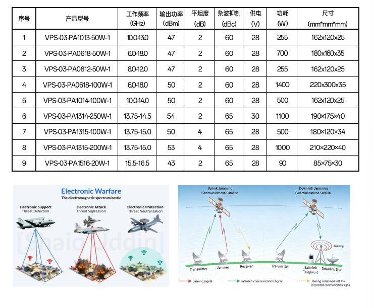
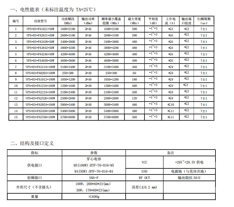
Counter-drone equipment’s core task is to jam or spoof a target drone’s remote control and data links so it loses control or deviates from course. From an RF perspective it is fundamentally a high-power wideband transmit system, with the technical difficulty concentrated in wideband amplifiers, high-power combining, transmit-receive isolation, and antenna systems.
A typical RF architecture has three sections. The jamming signal generation section produces baseband jamming waveforms (noise, swept, pulsed) from a DDS or FPGA with a high-speed DAC and upconverts them to the target band through a wideband quadrature modulator. The wideband driver and amplifier section amplifies through multiple wideband stages (driver plus final) to high power, from tens to hundreds of watts. The power combining and antenna section combines multiple amplifier outputs into one path through Wilkinson dividers and combiners or spatial combining, then feeds a high-gain directional antenna.
The key difference from the mesh datalink is that a datalink pursues low power, high sensitivity, and high linearity, while counter-drone equipment pursues high power, high efficiency, wide bandwidth, and thermal capacity. The design philosophies are entirely different.
4.2 Wideband Amplifier Design
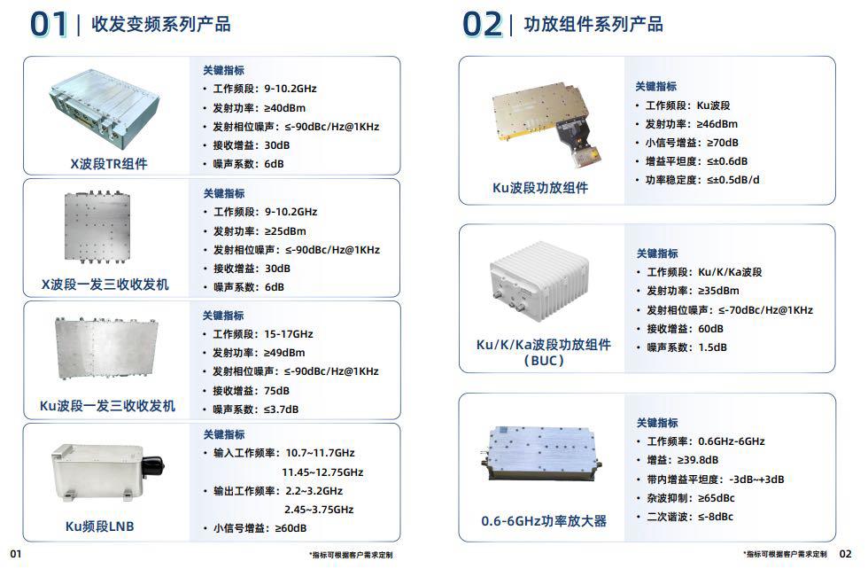
Low power, 1 to 5 W: two-stage cascaded GaAs PA MMICs, similar to the datalink amplifier approach. The emphasis is wideband matching using multi-section quarter-wave transformers or tapered lines to hold gain flatness across an octave.
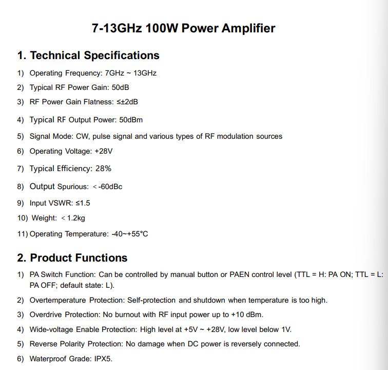
Medium power, 10 to 50 W: GaN MMICs or discrete GaN devices, where GaN’s advantages are decisive – power density five to ten times that of GaAs, high breakdown voltage for mismatch tolerance, good thermal conductivity, and high junction temperature capability above 200 degrees C. Domestic GaN vendors include CETC Institute 55, a leader in domestic GaN microwave devices with mature GaN HEMT and MMIC products in L through C band; Suzhou Innoscience for GaN epitaxy and devices; Dalian Xinguan for silicon-based GaN; Xiamen Sanan Integrated Circuit for GaN MMIC foundry and products; and Nanjing Guobo for GaAs and GaN RF MMICs.
For medium-power wideband amplifiers, push-pull or balanced architectures are recommended. A balanced design uses two amplifier MMICs with a 3 dB quadrature coupler, so the two amplifiers’ reflections cancel and input and output VSWR stay low across the whole band, with graceful degradation if one MMIC fails. In-band flatness and stability far exceed a single-ended design, making it the first choice for counter-drone amplifiers. Domestic 3 dB quadrature couplers can be built from lumped elements or microstrip, and microstrip couplers on high-frequency laminate perform well.
High power, above 100 W: power combining is mandatory. The usual approach is a Wilkinson divider and combiner splitting power into N paths, each amplified independently and then recombined. The critical Wilkinson specifications are isolation between paths and amplitude and phase balance – imbalance reduces combining efficiency and overloads individual amplifiers. The theoretical combining efficiency is 1/N times the per-path efficiency, so the split must be chosen deliberately. For ultra-wideband work, spatial combining such as radial waveguide combining is the more advanced route.
4.3 Transmit-Receive Isolation
Counter-drone equipment faces a problem the datalink does not: it must transmit high-power jamming while simultaneously receiving weak target signals for detection or jamming effectiveness assessment. Transmit power in the tens of watts against receiver sensitivity of -100 dBm is a difference of more than 140 dB, with the antennas perhaps only meters apart.
Five techniques, layered.
Antenna isolation: separate the transmit and receive antennas as far as possible, use high-gain directional antennas with sidelobes pointed away from the receive antenna, and add absorber material between them.
Time isolation: time division duplexing, with the receiver off during transmit and the transmitter off during receive, switched by fast RF switches in the microsecond range. GaAs RF switch MMICs can achieve this.
Frequency isolation: use different bands for transmit and receive with filters in between – a bandpass filter on the transmit side to suppress out-of-band leakage and one on the receive side to block the transmit frequency. High-rejection, low-insertion-loss cavity or dielectric filters are required.
Spatial isolation: keep transmit and receive paths physically separate on the PCB, separated by shielding walls, with no crossing traces.
Digital cancellation: a high-end technique. A coupler samples the transmit signal and a counter-phase signal is constructed digitally to cancel the leakage entering the receiver. It requires precise amplitude and phase calibration but can achieve cancellation depths beyond 40 dB.
4.4 Frequency Conversion Components
Conversion components are central to counter-drone and radar systems, upconverting low-frequency jamming waveforms or IF signals to the target RF band, or downconverting received RF to IF.
A typical upconversion chain: the baseband jamming signal from the FPGA and DDS passes through a quadrature modulator to the first IF (for example 70 MHz or a few hundred MHz); then an IF filter and VGA; then a mixer with the local oscillator upconverting to the target RF band; then an RF filter, driver amplifier, and final stage.
Three key design points. LO leakage suppression: the mixer leaks the local oscillator to the RF port, which is the main spurious source. Solutions include differential Gilbert cell mixers, balanced mixing with baluns, and an LO notch filter at the RF port, targeting LO leakage below -50 dBm. Sideband suppression: a quadrature modulator with I/Q imbalance produces unwanted sidebands, requiring digital calibration of gain and phase imbalance to within 0.1 dB and 1 degree. IF filter shape factor: the ratio of 60 dB bandwidth to 3 dB bandwidth determines adjacent channel rejection and should be below 1.5. Domestic SAW, crystal, and dielectric filters can meet this.
4.5 Advanced Wideband Matching: Octave and Ultra-Wideband
Conversion components often operate over very wide bands – an octave, 1 to 2 GHz, or 2 to 6 GHz. LC networks are insufficient and transmission line matching takes over.
Multi-section quarter-wave transformers: three to five quarter-wave microstrip sections at different impedances cascade to give flat matching across an octave, with section impedances distributed according to Chebyshev or binomial profiles. Chebyshev gives equal ripple in the passband with steep band-edge response; binomial is monotonic with a gentler edge. The former is wider, the latter smoother.
Klopfenstein taper: the impedance varies continuously along the length, giving theoretically unlimited bandwidth in practice limited by physical length.
Shunt and series stub matching: open or shorted microstrip stubs compensate device parasitic capacitance and inductance on the Smith chart, with stub lengths and positions optimized in electromagnetic simulation.
Distributed amplifiers: the ultimate ultra-wideband approach, treating device parasitic capacitance as part of an artificial transmission line and cascading multiple line sections for multi-octave bandwidth.
The key ultra-wideband specifications, restated: input and output VSWR below 2 across the band, in-band gain flatness within plus or minus 1 dB, full-band stability with the mu factor above 1, and harmonic suppression meeting target at every frequency. Satisfying all of these simultaneously is what makes a senior RF engineer valuable.
4.6 Radar RF Front Ends and T/R Modules
Radar RF components are more complex than datalinks or counter-drone systems because they handle transmit and receive simultaneously, often across many channels. The T/R module is the core element of an active phased array, with one module behind every antenna element.
A T/R module architecture: the transmit channel is a digitally controlled phase shifter, VGA, PA, and circulator or transmit-receive switch feeding the antenna; the receive channel is an LNA, VGA, attenuator, and phase shifter. The phase shifter is central because it determines beam pointing. Domestic 6-bit and 7-bit phase shifter MMICs from CETC Institutes 13 and 55 are mature, with phase accuracy within 2.8 degrees and amplitude error under 0.5 dB.
Key design points. Transmit-receive isolation via a circulator or RF switch. Amplitude and phase consistency: channel-to-channel amplitude and phase errors must be held within tight tolerances – amplitude under 0.5 dB and phase under 5 degrees – or beam pointing accuracy is lost. Thermal design: high T/R module density and high power make thermal management difficult, requiring thermal via arrays, thermal interface material, and cold plates.
For counter-UAV radar RF front ends, a very active area using small radars to detect low-altitude drones, the usual architecture is FMCW: the transmitter uses a VCO or PLL to generate a linear frequency ramp amplified and transmitted, while the receiver mixes the echo with the local oscillator to produce a difference-frequency IF signal, sampled by an ADC and FFT’d for range and velocity. Domestic DDS vendors include CETC Institute 24, Chengdu Huawei Microelectronics, and Beijing Shidai Minxin, with frequencies reaching hundreds of MHz to several GHz.
4.7 System-Level EMC and Layout
Chassis shielding: use a full metal enclosure, typically aluminum, with conductive treatment at all seams using conductive gaskets or beryllium copper fingers. Indicators, buttons, and vents on the panel need shielding through conductive film or metal mesh. SMA connectors must be well grounded.
Power filtering: the external 12 V input needs a common mode choke and X and Y capacitors for EMI filtering to prevent switching supply noise from radiating out through the power line.
Signal line filtering: the 100 Mbps Ethernet port needs a common mode choke with a Bob Smith termination (75 ohm resistors to ground plus 1000 picofarads to ground). Serial and USB ports need ESD protection devices.
Thermal design: calculate the PA thermal path explicitly – junction to case, case to heat sink, heat sink to ambient – and sum them to get junction temperature. Ensure it stays below the device maximum with 20 percent margin. GaN is typically rated 150 to 200 degrees C. Choose fin height and pitch appropriately, and use a fan for forced air cooling while watching fan EMI and vibration.
Grounding strategy: distinguish chassis ground, digital ground, analog ground, and RF ground, and join them at a single point. Shields connect to chassis ground, the DC supply negative connects to digital ground, and RF ground connects to chassis ground through a 0.01 microfarad capacitor for high-frequency return. Getting this right resolves most EMC problems.
4.8 Field Cases
Case one: a wideband amplifier for a portable counter-drone unit. The customer required 2 to 6 GHz ultra-wideband coverage, 100 MHz instantaneous bandwidth, 50 W output, efficiency above 40 percent, and total weight under 5 kg. The design used domestic GaN MMICs in the final stage with a balanced architecture (3 dB quadrature coupler plus two amplifier paths), a four-section Chebyshev quarter-wave transformer matching network, and high-frequency mixed laminate. The hard part was thermal: 50 W output at 40 percent efficiency means 75 W of dissipation. The solution combined thermal via arrays, a copper substrate, an aluminum heat sink, and a small fan, holding junction temperature under 120 degrees C. The biggest production pitfall was GaN threshold voltage batch dispersion, which produced 30 percent static current variation between batches. Automatic calibration – scanning each channel for its optimum bias point at power-up and storing it – solved the problem completely.
Case two: volume production of a mesh datalink. The requirements matched the opening of this article: 20 km, 40 ms, 33 dBm, fully domestic. The build used a domestic FPGA, a domestic RF transceiver, a domestic PA MMIC, a domestic power supply, and domestic passive components. In production, different batches of the PA MMIC differed by 2 dB in small-signal gain, causing 3 dB of output power variation across units. The fix was closed-loop power control: a directional coupler, detector, and ADC feeding the FPGA, which automatically adjusts the front-end digital step attenuator to lock output power at 33 dBm plus or minus 0.5 dB. That eliminated the batch consistency problem entirely. The lesson, worth repeating: production specifications cannot be guaranteed by component consistency. They must be guaranteed by closed-loop control in the circuit.
Case three: a T/R module for counter-UAV radar. Eight channels at 5.8 GHz, 10 W transmit per channel, 2 dB receive noise figure, and amplitude and phase consistency within 0.5 dB and 5 degrees. The build used domestic phase shifter MMICs, domestic PA MMICs, and domestic circulators in an eight-channel integrated module. The biggest challenge was multi-channel amplitude and phase consistency – individual channels met specification, but the eight channels differed by 1 dB and 10 degrees. Per-channel FPGA calibration, sweeping and compensating amplitude and phase errors at power-up, plus tight PCB fabrication tolerances (0.02 mm trace width tolerance, with dielectric constant dispersion absorbed by design margin) brought all eight channels into specification.
The common thread across all three: domestic devices were not the problem and the circuit design was not the problem. What is genuinely hard in production is batch dispersion and multi-channel consistency, and the answer is always closed-loop control and calibration.
Chapter 5: Prototype Debugging
5.1 The Debug Bench
Instruments are the RF engineer’s eyes and ears. Not knowing how to use them is equivalent to being blind.
Vector network analyzer (VNA). The single most important RF debugging instrument, measuring S-parameters (S11, S22, S21, S12), VSWR, return loss, impedance, and group delay. Domestic options include Ceyear (formerly Institute 41) AV3672 and AV3656 series covering to 20 GHz and beyond, Chengdu Jiujin’s VNA line, and Transcom VNAs. These are accurate enough from 1 to 6 GHz to be the first choice for domestic substitution.
Spectrum analyzer. For spectrum, power, spurious, harmonics, ACLR, and phase noise. Domestic options include Ceyear AV4032 and AV4036 series, Chengdu Jiujin, Transcom, and RIGOL at the low end. Real-time spectrum capability is better because it catches transient signals.
Signal generator. For single tones, modulated signals, and swept signals. Domestic options include Ceyear AV1443 and AV1464 series, Chengdu Jiujin, Transcom, and RIGOL.
Power meter and power sensor. More accurate than a spectrum analyzer for RF power. The sensor must cover the target band and power range – for example -60 to +20 dBm up to 6 GHz.
Noise figure analyzer. For measuring LNA and receive chain noise figure. Keysight N8975A at the high end, or domestic equivalents, or a gain-method (Y-factor) calculation using a spectrum analyzer.
Oscilloscope. For digital signals, clocks, supply ripple, and modulation waveforms. Domestic options include RIGOL DS70000 series to 5 GHz, SIGLENT, and UNI-T. At least 200 MHz bandwidth, preferably 1 GHz or more with MSO capability.
DC power supply. Programmable, multi-channel, low noise, with current display for power measurement. Domestic options include GW Instek, RIGOL, and ITECH.
Multimeter and LCR meter. For voltage, resistance, capacitance, and inductance.
Supporting tools: RF cables (semi-rigid and semi-flexible), adapters (SMA, N-type), attenuators (10, 20, and 30 dB for extending power meter and spectrum analyzer range), 50 ohm loads, VNA calibration standards (open, short, load, through), a thermal camera for temperature mapping, a reflow station or hot air gun, and a microscope for solder inspection.
The list looks expensive, but these instruments are the team’s livelihood – a one-time investment that lasts a decade. Every engineer should personally operate each instrument at least once and become familiar with the basic workflow, ranges, accuracy, and calibration procedure.
5.2 The Correct Power-Up Sequence
This is both the most exciting and the most damaging moment. Boards have been destroyed by connecting 12 V and switching on immediately.
Step one, visual inspection. Against the BOM and schematic, verify every device: designator, part number, orientation for diodes, tantalum capacitors, and ICs, and check for missing, extra, or wrong parts, solder balls, bridges, and cold joints. This catches more than half of all low-level errors.
Step two, multimeter measurement. Measure the impedance from each rail to ground – 12 V, 5 V, 3.3 V, 1.8 V, 1.2 V. Normal readings are several hundred ohms or more. A reading of a few ohms or a short means a failed device or a solder ball short, and power must not be applied. This step saves your power chips.
Step three, modular power-up. Do not connect all 12 V at once. Populate the power section first, power the supply module alone, and verify each output voltage and ripple (under 50 mV peak to peak). Then populate the digital section (FPGA, clock), power up, and confirm the clock oscillates and configuration responds. Then the RF transceiver, checking that it locks. Only then the power amplifier.
Step four, stage-by-stage tuning. Start the amplifier at small signal, never at full power. Check S-parameters on the VNA to confirm matching, then use a small signal source and power meter to check gain and output power, and only then increase input power to measure large-signal performance.
Step five, thermal watch. On the first high-power run, watch the PA and power devices on a thermal camera. If temperature climbs rapidly, reduce power or shut down and investigate cooling.
5.3 Output Power
Measurement: the signal source produces the target modulated signal (for example 64QAM at some megasymbols per second) and drives the amplifier input; the output goes through an attenuator (for example 30 dB, bringing 33 dBm down to 3 dBm, inside the instrument range) to the spectrum analyzer or power meter. The reading plus the attenuator value is the actual output power.
Calibrate first. The attenuator value should be verified on the VNA because attenuators have frequency response and VSWR of their own. The spectrum analyzer should be calibrated and set with the correct RBW (1 MHz suggested), VBW (3 MHz or more to smooth noise), reference level, and units (dBm).
Tuning: insufficient output can come from insufficient input power (check the preceding gain and attenuator setting), incorrect matching (check S22 on the VNA and tune the output match), incorrect bias (check quiescent current and raise bias if needed), or the amplifier already being in compression (check for overdrive). Excess spurious with adequate power means the amplifier is pushed too deep into saturation and needs more back-off.
Full-temperature test: measure output power at room, -20, and +60 degrees C. Variation with temperature should stay within plus or minus 1 dB. Larger drift points to bias temperature drift, corrected with a temperature-compensated bias circuit.
5.4 Efficiency
Efficiency determines endurance and thermal headroom. Two metrics matter: drain efficiency, the ratio of RF output power to DC input power, and power added efficiency, which is (RF output minus RF input) divided by DC input power and better reflects real efficiency.
Measurement: the DC supply must display current, or use a current meter in series. Measure supply voltage and current to get DC input power, and RF output power on the power meter. Where input power is measurable, use PAE; otherwise use drain efficiency.
Tuning: techniques include raising bias to operate deeper into saturation, at the cost of linearity; using a Doherty architecture, which maintains high efficiency in the back-off region by coordinating a main and an auxiliary amplifier; envelope tracking, where the supply voltage follows the signal envelope to hold efficiency high; and reducing matching network and transmission line loss through low-loss laminate and low-loss inductors.
For this project, 33 dBm output on a 12 V rail, the efficiency target is above 40 percent. That puts PA stage DC consumption near 5 W, total unit consumption around 10 W, and current near 0.8 A at 12 V – achievable with careful design.
5.5 Gain Flatness
Flatness is a key wideband specification: gain variation under plus or minus 0.5 dB across the whole operating band.
Measurement: sweep S21 on the VNA, or step through frequency with a signal source and spectrum analyzer. The sweep should cover the operating band plus 10 percent margin, with RBW narrow enough to catch detail.
Tuning: poor flatness means the matching network response is uneven at the band edges. Adjust the inductor and capacitor values in the matching network to flatten the response, apply pre-equalization in the digital domain through the FPGA with different gain compensation at different frequencies, or use a tunable equalizer in the RF domain.
One technique worth emphasizing: tune flatness at small signal in the linear region, not at maximum power. At high power the amplifier’s self-heating changes gain and the response varies with power. Get small-signal flatness right first, then verify at power.
5.6 Linearity: EVM and ACLR
Linearity determines whether 64QAM is usable and whether adjacent channels are interfered with. Two core metrics: EVM, requiring under 3 percent RMS with high-end products under 1 percent, and ACLR, requiring better than -45 dBc.
Measurement: a vector signal generator produces a standard modulated signal (for example 64QAM with 10 MHz bandwidth) driving the amplifier; the output passes through an attenuator to a vector signal analyzer, or a high-end spectrum analyzer with vector analysis, reading EVM and ACLR directly.
Tuning: insufficient linearity means the amplifier is pushed too deep into the nonlinear region. In priority order: back off by reducing input power to operate in a more linear region, at the cost of efficiency – the simplest and most effective fix; raise bias to move from class C toward class AB or class A, improving linearity at the cost of efficiency; apply digital predistortion in the digital domain to cancel the amplifier nonlinearity, which is the high-end approach because it allows the amplifier to be pushed harder while retaining linearity and significantly improves efficiency; or apply local negative feedback in the circuit.
In practice: use back-off to quickly identify the linear region and set the input power point; then use predistortion or bias adjustment at that point to bring EVM and ACLR inside specification; finally apply temperature compensation to hold linearity across the temperature range.
5.7 Harmonic and Spurious Suppression
Harmonics and spurious emissions are critical for EMC and type approval, and are the most common production failure.
Measurement: set the spectrum analyzer start frequency to zero or below the local oscillator, and the stop frequency to three to five times the operating frequency; use a wider RBW (1 to 3 MHz) for a fast sweep; leave adequate reference level headroom to prevent large-signal compression; and enable the preamplifier for small signals. Read the fundamental, then the second and third harmonics, local oscillator leakage, reference clock leakage, and switching supply spurs.
Typical requirements are second harmonic below -40 dBc and third harmonic below -30 dBc, though the actual limits depend on the band and the certification requirements for the product.
Tuning: the first move is an output low-pass filter, either lumped LC or microstrip, with the cutoff just above the operating band and well below the second harmonic, attenuating it by 20 to 30 dB. The second is optimizing the output match so the amplifier presents a high impedance at harmonic frequencies, suppressing them naturally through harmonic tuning. The third is shielding, because sometimes port harmonics measure fine while enclosure seams still radiate and the EMC test still fails.
Spurious sources are varied: clock harmonics, PLL spurious, reference crystal harmonics, digital crosstalk, and switching supply frequencies. Use a near-field probe with a spectrum analyzer to scan the board point by point, locate the radiator, then apply targeted filtering, shielding, and ground vias.
5.8 Receive Chain: Noise Figure and Sensitivity
The receive chain’s core metrics are noise figure and sensitivity, which determine how weak a signal can be received.
Measurement: measure directly with a noise figure analyzer, or use the gain method – inject a single tone of known power, measure output power on the spectrum analyzer to derive gain, then measure output noise power to calculate noise figure.
Tuning: if noise figure is out of specification, check that the LNA is operating correctly (bias and gain), check the loss ahead of the LNA since connector, switch, and filter insertion loss adds directly to the noise figure, and check local oscillator phase noise, which limits sensitivity at close-in offsets.
Sensitivity test: use a vector signal source to generate a modulated signal and reduce power until the demodulated BER or SNR reaches threshold – for example BER of 10^-6 – at which point the input power is the sensitivity. The target is better than -105 dBm at 10 MHz bandwidth.
5.9 Local Oscillator and Clock Debugging
Three things to check: lock time, phase noise, and spurious.
Lock time: view the phase detector lock detect signal and the reference clock on an oscilloscope; the interval from lock enable to lock detect going high is the lock time. Millisecond performance is required. Slow locking points to a narrow loop bandwidth or incorrect loop filter values.
Phase noise: measure at 1 kHz, 10 kHz, 100 kHz, and 1 MHz offsets. Poor close-in phase noise degrades receive sensitivity; poor far-out phase noise degrades adjacent channel selectivity.
Optimizing phase noise: widen the loop bandwidth so close-in noise tracks the reference, use a low-phase-noise reference clock such as a TCXO or OCXO, filter and shield the VCO tuning line, and keep the supply clean with LDOs and multi-stage decoupling.
Spurious: the PLL phase detector frequency leaks to the output as discrete spurs spaced at the phase detector frequency. Suppress them with adequate loop filter attenuation (third order or higher), a phase detector frequency chosen well away from the band of interest, and fractional-N spurious suppression techniques where needed.
5.10 System Integration and Waveform Reading
System integration is the most demanding stage, connecting every module end to end and observing overall behavior.
Steps: baseband self-test with the FPGA generating test data and looping internally to confirm baseband logic; RF loopback, feeding the transmit chain output back to the receive chain through an attenuator to confirm both paths work; over-the-air testing between two units measuring BER, throughput, and range; and stress testing with temperature cycling, vibration, and extended aging.
Waveform reading is a craft. A few typical cases and what they mean.
QPSK, 16QAM, or 64QAM on a spectrum analyzer should appear as a broadband grass-like spectrum with a smooth envelope, flat in-band response, and fast out-of-band roll-off. Spikes indicate single-tone spurious; in-band ripple indicates a power amplifier or filter response problem; a shallow roll-off indicates a poor filter shape factor.
Constellation diagrams should show four distinct points for QPSK, sixteen for 16QAM, and sixty-four for 64QAM. Points smeared into a cloud indicate poor SNR or amplifier nonlinearity; points offset from center indicate I/Q DC offset; points distributed in an arc indicate I/Q amplitude or phase imbalance.
Baseband I/Q waveforms should show a smoothly varying envelope. Ringing indicates impedance mismatch or reflection; overshoot indicates excessive bandwidth or parasitic inductance; periodic ripple on the supply indicates switching supply noise coupling in.
Thermal images should show the PA and power devices as the hottest regions, but with even distribution. A localized hot spot indicates insufficient thermal vias or a blocked thermal path; temperature that keeps climbing without settling indicates a fundamental cooling design problem.
Reading these waveforms together lets an experienced RF engineer localize a problem in minutes. That skill comes only from practice and accumulated exposure.
Chapter 6: From Prototype to Mass Production
6.1 PCB Fabrication
Communication with the board house determines board quality.
Choosing a board house: there are many domestic options, including high-end suppliers and a large number of small and mid-sized houses. RF boards should go to a house that can handle high-frequency mixed lamination, impedance control, and laser drilling – more expensive but stable. Build an approved vendor list of two to three qualified suppliers as mutual backups.
Submitting data: the Gerber set must be complete – each layer’s traces, silkscreen, solder mask, paste mask for the stencil, drill files, board outline, and a process specification covering stackup, material type, board thickness, copper weight, surface finish, impedance requirements, and solder mask color. State clearly: material (for example mixed Shengyi S7136H with FR-4), layer count, board thickness (1.2 mm), copper weight (1 oz outer, 0.5 oz inner), surface finish (ENIG or HASL), impedance requirements (50 ohm microstrip, 100 ohm differential), and special requirements such as impedance coupons and impedance test reports.
Impedance control is the lifeblood of an RF board. The board house must include an impedance coupon and attach measured impedance values to the shipping report. If measured deviation exceeds plus or minus 10 percent, the batch is rejected and remade. This belongs in the contract.
Prototype rounds: three rounds are recommended – engineering samples of 5 to 10 pieces to verify feasibility, design verification of 20 to 50 pieces, and a pilot run of 100 to 200 pieces to validate production processes. Each round needs complete test records and a trial production report.
Incoming inspection: check appearance (copper, solder mask, silkscreen, barrel quality), dimensions (outline, hole sizes), impedance (sampling the coupon), solderability (wetting test), and warp (under 0.75 percent). Reject the whole batch if it fails.
6.2 Mechanical Parts and Surface Treatment
Material selection: aluminum alloy 6063-T5 for extruded heat sinks or 5052 sheet for enclosures. Weight-sensitive designs can use magnesium alloy such as AZ31, at higher cost and machining difficulty. RF shielding cavities can use stamped nickel silver for the best shielding effectiveness.
Processes: CNC machining for small batches and complex geometry, die casting for volume where tooling cost is amortized, and sheet metal for enclosures and brackets. CNC is sufficient for small-batch projects.
Surface treatment: aluminum should be hard anodized at 20 to 30 micrometers, in the customer’s color. Anodizing both protects and insulates, but note that the anodized surface is non-conductive, so the conductive path between enclosure and PCB ground needs conductive chromate conversion or conductive gaskets. Shields should be nickel or tin plated for good conductivity.
Heat sink design: fin height and pitch follow the cooling mode. Typically 20 to 40 mm fin height and 3 to 5 mm pitch. Run a thermal simulation to confirm airflow and temperature distribution.
Inspection: dimensional accuracy on a CMM, surface roughness under Ra 1.6 micrometers, anodize thickness with an eddy current gauge, and interference checking by physical assembly.
6.3 Assembly and Soldering
Stencil: stencil thickness and aperture size determine solder volume. RF devices, especially power MMICs with thermal pads, need special treatment – the thermal pad aperture should be gridded or slotted to prevent too much solder and device float, while the small surrounding pins use rounded rectangular apertures to prevent solder balls. Stencil thickness is typically 0.12 to 0.15 mm.
Solder paste: lead-free SAC305 with a melting point of 217 degrees C. Watch the shelf life (six months) and refrigeration requirement (0 to 10 degrees C), and allow four hours of warming and stirring before use.
Placement: generate the machine program from the centroid file and BOM, load materials per the feeder list, and set the reflow profile strictly per the paste specification – ramp of 1 to 3 degrees C per second, soak at 150 to 200 degrees C for 60 to 120 seconds, reflow above 217 degrees C with a peak of 235 to 245 degrees C for 30 to 60 seconds, and cooling at 1 to 4 degrees C per second. Peak temperature must not be too high or both devices and board will be damaged.
Solder inspection: AOI for wrong, missing, or reversed components and bridges and cold joints; X-ray for bottom-terminated pads on BGAs, QFNs, and power MMIC thermal pads. This last check is critical for RF power amplifiers – a poorly soldered thermal pad raises thermal resistance, overheats the device, and destroys both performance and reliability.
Hand soldering and rework: hot air gun temperature should not be excessive (320 to 350 degrees C), time should be short (under 3 seconds per pin), and ESD grounding is essential. For power MMICs, apply flux, heat evenly, and clean flux residue with isopropyl alcohol afterward.
Assembly order: small components first (resistors, capacitors, inductors), then medium devices (ICs, connectors), then large and thermal parts. Power MMICs go last because they are static- and temperature-sensitive. Clean the board after soldering – ultrasonic or manual – to remove flux residue, which absorbs moisture and leaks current in humid conditions, causing specification drift.
6.4 Prototype Debugging and Testing
Process: module-by-module debugging of supply, clock, baseband, transceiver, PA, and receive chain; full system integration to measure end-to-end specifications; environmental testing for temperature, vibration, shock, damp heat, and aging; and pre-compliance EMC scanning in an anechoic chamber to catch problems early.
Records: every prototype needs a complete test file – debugging log, specification test report, and fault and resolution record. All test data should record raw values, computed values, and conclusions. This is the basis for production problem traceability.
Design freeze: after all prototype tests pass, issue a design verification report confirming all specifications and freeze the design. Any change afterward goes through the ECN process. This is production discipline.
6.5 Production Introduction and Consistency Control
Three core production problems: device batch dispersion, process variation (solder volume, placement accuracy, reflow profile), and assembly consistency (mechanical parts, thermal contact). These stack and spread the specification distribution. Five controls address them.
Control one: critical device locking and normalization. Sign long-term supply agreements for critical devices – PA MMICs, LNAs, FPGAs, crystals, and key inductors and capacitors – locking part number, package, batch, and test conditions. Each critical device needs a defined normalized parameter range, with out-of-range batches screened or compensated.
Control two: process freeze and statistical process control. Freeze reflow profiles, placement accuracy, stencil apertures, and cleaning into standard operating procedures. Run SPC on critical steps such as PA soldering, shield assembly, and heat sink mounting, recording mean and standard deviation of key parameters like solder thickness, contact thermal resistance, and shield gap, with alarms beyond three sigma.
Control three: closed-loop calibration. Design adjustable elements into the circuit – digital step attenuators, adjustable bias, tunable equalizers – measure the deviation at final test, compute the compensation with the FPGA or MCU, and write it to EEPROM or flash for automatic loading at power-up. Every unit is then calibrated to its own optimum and device dispersion is cancelled out.
Control four: automated test equipment. Manual tuning is too slow and too inconsistent for volume. Build an ATE that drives the spectrum analyzer, power meter, VNA, and DC supply over GPIB or LXI, running the test sequence automatically, judging pass or fail, and generating reports. The investment pays back above 100 units and lifts consistency beyond what manual testing can reach.
Control three through five together form the backbone of production consistency: burn-in screening at maximum operating temperature and rated voltage for 24 to 48 hours to remove early failures, with specifications measured before and after and out-of-tolerance drift rejected; and temperature cycling from -40 to +85 degrees C over dozens of cycles to screen out soldering and material defects. These are standard quality gates for industrial and defense equipment.
6.6 Diagnosing Batch-Level Specification Drift
This is the most valuable skill a senior engineer has. A standard procedure.
Step one, build a distribution. Plot the batch’s specification data as a histogram. A whole-distribution shift points to a systematic cause such as a changed design or process parameter; scatter points to a random cause such as device dispersion or assembly variation.
Step two, stratify. Break the data down by batch, supplier, and process step to find where the anomaly concentrates. If only units with a particular PA MMIC batch run low, it is a device batch problem. If only units built on a particular day are affected, it is a process excursion that day.
Step three, fishbone analysis. Work through the six dimensions – people, machine, material, method, environment, and measurement. Was the operator following procedure? Was the equipment calibrated? Were material batches consistent? Did process parameters drift? Were temperature and humidity abnormal? Was the test method or instrument consistent?
Step four, verify the hypothesis. Run a controlled A/B comparison – change one device batch, one process step, or one parameter – and see whether the specification returns. Change only one variable at a time or attribution is impossible.
Step five, institutionalize the countermeasure. Write the countermeasure into the design specification or the work instruction to prevent recurrence. This closing step is the most commonly skipped.
Two real examples. A batch failed second harmonic limits; investigation found a board house batch with thin dielectric, which lowered microstrip impedance, detuned the output match, dropped the amplifier’s harmonic-frequency impedance, and reduced harmonic suppression. The countermeasure was adding dielectric thickness and constant dispersion to incoming inspection and designing matching networks with margin against laminate parameters. Another batch drifted 2 dB in power across temperature; the cause was an ordinary X7R capacitor used for loop filtering in the bias circuit, whose temperature coefficient shifted the bias voltage. The countermeasure was switching that capacitor to C0G and adding temperature-compensated bias. The lesson: production problems are eight times out of ten caused by details someone considered unimportant.
6.7 Documentation and Traceability
Required documents: design input (requirements, specifications); design output (schematic, PCB, BOM, mechanical drawings, software code); design verification (test reports, trial production reports, problem lists with closure records); engineering change notifications recording requester, reason, impact analysis, verification, and approval; material management (approved vendor list, material specifications, batch records); production management (SOPs, process cards, first article confirmation, inspection reports); and quality records (incoming, in-process, and outgoing inspection, burn-in records, and fault statistics).
Traceability: every unit needs a unique serial number linking its material batches, production steps, test data, and inspection records. Problems must be traceable to an individual device, an individual solder joint, and an individual test. This is a baseline requirement for defense equipment.
6.8 Closing Notes
Five things worth remembering. First, RF engineering is a craft, and craft comes from practice, not from reading – handle boards, use instruments, and yes, destroy components; the more you destroy, the faster you learn. Second, detail is the soul of RF; a single via, capacitor, or trace can decide whether the unit works. Third, do not trust datasheets blindly – they give typical values, while production depends on distributions and tolerances. Fourth, domestic sourcing is an opportunity, not a compromise; domestic RF devices have improved visibly and world-class products are already being built. Fifth, compliance is the floor and a mark of professionalism.
Now go and do the work. The board is waiting to be laid out, the amplifier is waiting to be tuned, and the line is waiting to be run. Every specification met is a mark of your craft.
Mesh VTX Design Parameters at a Glance
| Parameter | Target | Design implication |
|---|---|---|
| Center frequency | 1400 MHz (L-band example) | 121.4 dB free-space loss at 20 km |
| Range | 20 km line of sight | 20.6 dB margin before real-world losses |
| Transmit power | 33 dBm (2 W) | Drives PA, thermal, and supply design |
| End-to-end latency | Under 40 ms | Under 10 ms from RF and baseband, 30 ms for the stack |
| Modulation | Adaptive QPSK / 16QAM / 64QAM | Requires dynamic bias control |
| Supply | 12 V DC, roughly 1 A | Wide power traces, heavy decoupling |
| Operating temperature | -20 to +60 degrees C | Full-temperature device screening |
| Receiver sensitivity | Better than -105 dBm at 10 MHz BW | Low noise figure LNA, low phase noise LO |
| Linearity | EVM under 3 percent RMS, ACLR under -45 dBc | Back-off or digital predistortion |
| PCB | 6 layers, mixed high-frequency laminate | 1.2 mm thick, 50 ohm microstrip |
Have questions about this article? Feel free to contact us at [email protected] — we’re happy to help!
Frequently Asked Questions
Why is a 20 km link budget so sensitive to small losses?
Because path loss scales with distance logarithmically while the available margin is small. At 1400 MHz the 20 km path costs 121.4 dB, leaving about 20.6 dB of margin on a 33 dBm transmitter – and antenna misalignment, feed loss, and multipath consume most of it.
Why must the link budget be built with worst-case columns?
Margin is consumed by effects that occur together in the field – high temperature, low supply voltage, and antenna mismatch can all happen at once. A design validated only at nominal values will pass on the bench and fail in volume production.
Why are C0G capacitors required in RF matching networks?
C0G has a temperature coefficient near zero and no DC bias effect, so capacitance does not shift with operating voltage. An X7R part under 12 V bias can lose half its nominal value, which changes the impedance and detunes the match.
What is the difference between an L-match and a quarter-wave transformer?
An L-match uses lumped reactances and suits narrowband designs with moderate transformation ratios. A quarter-wave transformer uses a transmission line section and, in multi-section form, covers an octave or more with flat response – necessary when lumped element Q and power handling fall short.
How is production consistency actually achieved?
Through closed-loop calibration, not component tolerance. The circuit includes adjustable elements, final test measures the deviation, and the compensation value is written to memory and loaded at power-up so each unit is calibrated to its own optimum.
About Aomway
Aomway is a technology company specializing in drone and FPV equipment, publishing in-depth analyses of motor control, embedded hardware, and open-source robotics projects. With over 15 years of industry experience, Aomway covers the full spectrum from flight controllers and FPV goggles to thermal imaging cameras and long-range datalinks for the global drone community.